CD4053BCM Fairchild Semiconductor, CD4053BCM Datasheet
CD4053BCM
Specifications of CD4053BCM
Available stocks


Related parts for CD4053BCM


CD4053BCM Summary of contents
Page 1
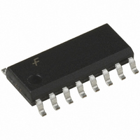
... M16D 16-Lead Small Outline Package (SOP), EIAJ TYPE II, 5.3mm Wide CD4052BCN N16E 16-Lead Plastic Dual-In-Line Package (PDIP), JEDEC MS-001, 0.300 Wide CD4053BCM M16A 16-Lead Small Outline Integrated Circuit (SOIC), JEDEC MS-012, 0.150 Narrow CD4053BCSJ M16D 16-Lead Small Outline Package (SOP), EIAJ TYPE II, 5.3mm Wide ...
Page 2
Connection Diagrams Pin Assignments for DIP and SOIC CD4051BC Truth Table INPUT STATES INHIBIT *Don’t Care condition. www.fairchildsemi.com CD4052BC CD4053BC “ON” ...
Page 3
Logic Diagrams CD4051BC CD4052BC 3 www.fairchildsemi.com ...
Page 4
Logic Diagrams (Continued) www.fairchildsemi.com CD4053BC 4 ...
Page 5
Absolute Maximum Ratings DC Supply Voltage ( Input Voltage ( Storage Temperature Range ( Power Dissipation ( Dual-In-Line Small Outline Lead Temperature ( (soldering, 10 ...
Page 6
DC Electrical Characteristics Symbol Parameter Conditions V LOW Level Input Voltage all OFF Channels 10V DD V 15V DD V HIGH Level ...
Page 7
AC Electrical Characteristics ns, unless otherwise specified Symbol Parameter t Propagation Delay Time from V PZH Inhibit to Signal Output R PZL L (channel turning on ...
Page 8
Special Considerations In certain applications the external load-resistor current may include both V and signal-line components avoid drawing V current when switch current flows into DD IN/OUT pin, the voltage drop across the bidirectional Typical Performance Characteristics “ON” ...
Page 9
Switching Time Waveforms 9 www.fairchildsemi.com ...
Page 10
Physical Dimensions inches (millimeters) unless otherwise noted 16-Lead Small Outline Integrated Circuit (SOIC), JEDEC MS-012, 0.150 Narrow www.fairchildsemi.com Package Number M16A 10 ...
Page 11
Physical Dimensions inches (millimeters) unless otherwise noted (Continued) 16-Lead Small Outline Package (SOP), EIAJ TYPE II, 5.3mm Wide Package Number M16D 11 www.fairchildsemi.com ...
Page 12
Physical Dimensions inches (millimeters) unless otherwise noted (Continued) 16-Lead Thin Shrink Small Outline Package (TSSOP), JEDEC MO-153, 4.4mm Wide www.fairchildsemi.com Package Number MTC16 12 ...
Page 13
Physical Dimensions inches (millimeters) unless otherwise noted (Continued) 16-Lead Plastic Dual-In-Line Package (PDIP), JEDEC MS-001, 0.300 Wide Fairchild does not assume any responsibility for use of any circuitry described, no circuit patent licenses are implied and Fairchild reserves the right ...