MM74HC4053M Fairchild Semiconductor, MM74HC4053M Datasheet
MM74HC4053M
Manufacturer Part Number
MM74HC4053M
Description
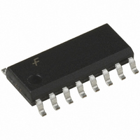
IC MUX/DEMUX TRIPLE 2X1 16SOIC
Manufacturer
Fairchild Semiconductor
Series
74HCr
Specifications of MM74HC4053M
Function
Multiplexer/Demultiplexer
Circuit
3 x 2:1
On-state Resistance
100 Ohm
Voltage Supply Source
Dual Supply
Voltage - Supply, Single/dual (±)
±2 V ~ 6 V
Current - Supply
16µA
Operating Temperature
-40°C ~ 85°C
Mounting Type
Surface Mount
Package / Case
16-SOIC (0.154", 3.90mm Width)
Number Of Channels
3 Channel
On Resistance (max)
230 Ohms
Propagation Delay Time
60 ns
On Time (max)
355 ns
Off Time (max)
290 ns
Supply Voltage (max)
6 V
Supply Voltage (min)
2 V
Maximum Power Dissipation
500 mW
Maximum Operating Temperature
+ 85 C
Minimum Operating Temperature
- 40 C
Mounting Style
SMD/SMT
Number Of Switches
Triple
Lead Free Status / RoHS Status
Lead free / RoHS Compliant
Available stocks
Company
Part Number
Manufacturer
Quantity
Price
Company:

Part Number:
MM74HC4053M
Manufacturer:
Fairchild Semiconductor
Quantity:
1 833
Part Number:
MM74HC4053M
Manufacturer:
FAIRCHILD/仙童
Quantity:
20 000
Company:
Part Number:
MM74HC4053M1R
Manufacturer:
ST
Quantity:
1 339
Part Number:
MM74HC4053MX
Manufacturer:
FAIRCHILD/仙童
Quantity:
20 000


© 1999 Fairchild Semiconductor Corporation
MM74HC4051M
MM74HC4051WM
MM74HC4051SJ
MM74HC4051MTC
MM74HC4051N
MM74HC4052M
MM74HC4052WM
MM74HC4052SJ
MM74HC4052MTC
MM74HC4052N
MM74HC4053M
MM74HC4053WM
MM74HC4053SJ
MM74HC4053MTC
MM74HC4053N
MM74HC4051 • MM74HC4052 • MM74HC4053
8-Channel Analog Multiplexer •
Dual 4-Channel Analog Multiplexer •
Triple 2-Channel Analog Multiplexer
General Description
The MM74HC4051, MM74HC4052 and MM74HC4053
multiplexers are digitally controlled analog switches imple-
mented in advanced silicon-gate CMOS technology. These
switches have low “on” resistance and low “off” leakages.
They are bidirectional switches, thus any analog input may
be used as an output and vice-versa. Also these switches
contain linearization circuitry which lowers the on resis-
tance and increases switch linearity. These devices allow
control of up to 6V (peak) analog signals with digital con-
trol signals of 0 to 6V. Three supply pins are provided for
V
5V logic signals when V
of 5V when V
inhibit control which when HIGH will disable all switches to
their off state. All analog inputs and outputs and digital
inputs are protected from electrostatic damage by diodes
to V
MM74HC4051: This device connects together the outputs
of 8 switches, thus achieving an 8 channel Multiplexer. The
binary code placed on the A, B, and C select lines deter-
mines which one of the eight switches is “on”, and con-
nects one of the eight inputs to the common output.
Ordering Code:
Devices also available in Tape and Reel. Specify by appending the suffix letter “X” to the ordering code.
Order Number
CC
CC
, ground, and V
and ground.
EE
Package Number
EE
5V. All three devices also have an
. This enables the connection of 0–
CC
MTC16
MTC16
MTC16
M16A
M16B
M16D
M16A
M16B
M16D
M16A
M16B
M16D
N16E
N16E
N16E
5V and an analog input range
16-Lead Small Outline Integrated Circuit (SOIC), JEDEC MS-012, 0.150” Narrow
16-Lead Small Outline Integrated Circuit (SOIC), JEDEC MS-013, 0.300” Wide
16-Lead Small Outline Package (SOP), EIAJ TYPE II, 5.3mm Wide
16-Lead Thin Shrink Small Outline Package (TSSOP), JEDEC MO-153, 4.4mm Wide
16-Lead Plastic Dual-In-Line Package (PDIP), JEDEC MS-0010.300” Wide
DS005353.prf
MM74HC4052: This device connects together the outputs
of 4 switches in two sets, thus achieving a pair of 4-channel
multiplexers. The binary code placed on the A, and B
select lines determine which switch in each 4 channel sec-
tion is “on”, connecting one of the four inputs in each sec-
tion to its common output. This enables the implementation
of a 4-channel differential multiplexer.
MM74HC4053: This device contains 6 switches whose out-
puts are connected together in pairs, thus implementing a
triple 2 channel multiplexer, or the equivalent of 3 single-
pole-double throw configurations. Each of the A, B, or C
select lines independently controls one pair of switches,
selecting one of the two switches to be “on”.
Features
Wide analog input voltage range: 6V
Low “on” resistance:
50 typ. (V
30 typ. (V
Logic level translation to enable 5V logic with 5V ana-
log signals
Low quiescent current: 80 A maximum (74HC)
Matched Switch characteristic
Package Description
CC
CC
–V
–V
EE
EE
4.5V)
9V)
August 1984
Revised May 1999
www.fairchildsemi.com
Related parts for MM74HC4053M
Image
Part Number
Description
Manufacturer
Datasheet
Request
R

Part Number:
Description:
Fairchild Semiconductor [IGBT MODULE]
Manufacturer:
Fairchild Semiconductor
Datasheet:

Part Number:
Description:
Discrete Semiconductor Modules
Manufacturer:
Fairchild Semiconductor
Part Number:
Description:
Discrete Semiconductor Modules
Manufacturer:
Fairchild Semiconductor
Part Number:
Description:
This N-Channel MOSFET is produced using Fairchild Semiconductor�s advanced Power Trench� process
Manufacturer:
Fairchild Semiconductor
Datasheet:
Part Number:
Description:
This N-Channel MOSFET is produced using Fairchild Semiconductor�s advanced Power Trench� process
Manufacturer:
Fairchild Semiconductor
Datasheet:
Part Number:
Description:
This N-Channel MOSFET is produced using Fairchild Semiconductor�s advanced PowerTrench� process
Manufacturer:
Fairchild Semiconductor
Datasheet:
Part Number:
Description:
This N-Channel MOSFET is produced using Fairchild Semiconductor�s advanced PowerTrench� process
Manufacturer:
Fairchild Semiconductor
Datasheet:
Part Number:
Description:
This N-Channel MOSFET is produced using Fairchild Semiconductor�s advanced Power Trench� process
Manufacturer:
Fairchild Semiconductor
Datasheet:
Part Number:
Description:
This N-Channel logic Level MOSFETs are produced using Fairchild Semiconductor�s advanced Power Trench� process that has been special tailored to minimize the on-state resistance and yet maintain superior switching performance
Manufacturer:
Fairchild Semiconductor
Datasheet:
Part Number:
Description:
This N-Channel MOSFET is produced using Fairchild Semiconductor�s advanced Power Trench� process
Manufacturer:
Fairchild Semiconductor
Datasheet:
Part Number:
Description:
This N-Channel SyncFET� is produced using Fairchild Semiconductor�s advanced PowerTrench� process
Manufacturer:
Fairchild Semiconductor
Datasheet:
Part Number:
Description:
This N-Channel SyncFET� is produced using Fairchild Semiconductor�s advanced PowerTrench� process
Manufacturer:
Fairchild Semiconductor
Datasheet:
Part Number:
Description:
This N-Channel SyncFET� is produced using Fairchild Semiconductor�s advanced PowerTrench� process
Manufacturer:
Fairchild Semiconductor
Datasheet:
Part Number:
Description:
This N-Channel logic Level MOSFETs are produced using Fairchild Semiconductor�s advanced Power Trench� process that has been special tailored to minimize the on-state resistance and yet maintain superior switching performance
Manufacturer:
Fairchild Semiconductor
Datasheet: