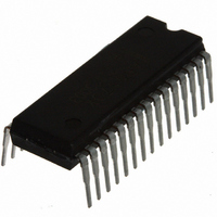
AN5870K Panasonic - SSG, AN5870K Datasheet

AN5870K
Specifications of AN5870K
Available stocks
Related parts for AN5870K
AN5870K Summary of contents
Page 1
... ICs for TV AN5870K Wide bandwidth analog switch IC I Overview The AN5870K is a wide bandwidth analog switch IC of 300 MHz operation usable for RGB signal and horizontal/vertical synchronizing signals, and it has a built-in 75 driver for video signal. In addition, it has also realized a high speed operation by the adoption of CMOS process for its sync ...
Page 2
... AN5870K I Block Diagram 1 R-in1 2 GND (R) 3 R-in2 CC1 5 G-in1 6 GND (G) 7 G-in2 CC1 9 B-in1 10 GND (B) 11 B-in2 CC1 13 H-in1 14 H-in2 15 V-in1 select bias Sync. sep Hsync detect sw SDB00035BEB 30 V (12 V) CC2 29 R-out 28 V CC2 27 G-out 26 GND ( sync. 24 GND ( B-out Sync Pdet. ...
Page 3
... CC2 I (pin 4, pin 8, pin 12) CC1 I (pin 28, pin 30) CC2 opr T stg Symbol V CC1 V 10.5 to 12.6 CC2 SDB00035BEB AN5870K Description V input 2 GND (HV, HSEP, SW) V output H output H detect Sync. input SW B output GND (RGB) G sync. output GND (RGB) G output (RGB) CC2 R output (RGB) CC2 Rating 5 ...
Page 4
... AN5870K I Electrical Characteristics at T Parameter Power supply Supply current (1) Supply current (2) Signal processing system Input DC voltage 1 Input DC voltage 2 Output DC voltage 1 Output DC voltage 2 Output DC voltage 3 Input impedance (1) Input impedance (2) Output impedance (1) Output impedance (2) Gain (1) Relative gain (1) Gain (2) Relative gain (2) Gain (3) Frequency characteristics 1 ...
Page 5
... V2 f Pin 22 difference form value C3 at 1MHz, pins SG5 signal, pins 23, 27, 29: Measurement f Relative difference Pin 22 difference form value MHz, pins 3, 7, 11: SG5 signal, pins 23, 27, 29: Measurement SDB00035BEB AN5870K Min Typ Max Unit 4.5 5.0 V 4.5 5.0 V 0.0 0.5 V 0.0 0 ...
Page 6
... AN5870K I Electrical Characteristics at T Parameter Signal processing system (continued) Relative frequency characteristics 4 (300 MHz) G-sync. frequency characteristics f (35 MHz) Relative gain between 2 inputs Relative frequency characteristics between 2 inputs (1) Relative frequency characteristics between 2 inputs (2) Crosstalk between RGB 3 (100 MHz) Crosstalk between RGB 4 ...
Page 7
... SG6 signal, pin 22 Pin 18 or 19: Measurement O3 t Pin 21: SG7 signal, r(SY) pin 19: Measurement t Pin 21: SG7 signal, f(SY) pin 19: Measurement t Pin 21: SG7 signal, rD(SY) pin 19: Measurement t Pin 21: SG7 signal, fD(SY) pin 19: Measurement I Pin 21 pin 21 sink current value S1 measurement SDB00035BEB AN5870K Min Typ Max Unit ...
Page 8
... AN5870K I Electrical Characteristic (continued) Input signal for testing Name Sine wave (f 1 MHz, amplitude 1 V[p-p]) SG1 SG2 Sine wave (f 10 MHz, amplitude 1 V[p-p]) SG3 Sine wave (f 35 MHz, amplitude 1 V[p-p]) SG4 Sine wave (f 100 MHz, amplitude 1 V[p-p]) SG5 Sine wave (f 300 MHz, amplitude 1 V[p-p]) Square wave (f 62 ...
Page 9
... Input through a capacitor GND pin for 5 V: For B signal circuit B signal input pin 2: Input through a capacitor Power supply pin for • Sync. separation • For SW circuit SDB00035BEB AN5870K Pin voltage (V) Input with sync. signal (typ.) 1.0 V[p-p] DC 2.9 V GND Input with sync. signal (typ ...
Page 10
... AN5870K I Terminal Equivalent Circuits (continued) Pin No. Equivalent circuit 13 Pins 13, Pins 14, Refer to pin 13 16 Refer to pin Description H. sync. signal input pin (pin 12 500 H. sync. signal input pin (pin 12 500 V sync. signal output pin 1: V sync. signal output pin 2: GND pin for • ...
Page 11
... B signal output pin: • Be sure to connect a capacitor to output pin. If the pin is not used with a 75 terminating resistor, do not allow more 220 F output current flow 0.01 F SDB00035BEB AN5870K Pin voltage (V) When detecting high-level (typ.) 2.5 V Sync. signal (typ.) 0.3 V[p-p] DC 1. (typ.) High-level ...
Page 12
... AN5870K I Terminal Equivalent Circuits (continued) Pin No. Equivalent circuit (pin 2 Refer to pin Refer to pin Description GND pin for 12 V Sync. on green signal Output pin: • If terminating with a resistor, do not allow more output current flow. 25 • For RGB signal circuit For G sync. output G signal output pin: • ...
Page 13
... H-out pin (pin 19 (state of sync.-in pin (H-in signal is selected exceeded) (Detection voltage change) 1V 2.5V H-in signal selection 3V SDB00035BEB AN5870K Output signal H-in signal Sync.in signal H-in signal H. sync. signal detection pin voltage 4V H. sync. signal detection pin voltage (Sync.-in signal is selected when exceeded) ...
Page 14
... AN5870K I Usage Notes 1. About C22 0.01 F capacitor (refer to I Application Circuit Example) In the case of evaluation board for this IC without heat sink, a resonance phenomena takes place at approx. 400 MHz between pin 23 B-out pin and pin 22 SW pin and affects the frequency characteristic of B-out pin. ...
Page 15
... I New Package Dimensions (Unit: mm) SDIP030-P-0400B (Lead-free package) 26. 1.778 (0.894) ±0. +0.10 0.50 -0.05 +0.10 0.70 -0.05 +0.10 0.90 -0.05 Seating plane SDB00035BEB AN5870K 10. ...
Page 16
Request for your special attention and precautions in using the technical information and semiconductors described in this material (1) An export permit needs to be obtained from the competent authorities of the Japanese Govern- ment if any of the products ...


