AD8184ARZ Analog Devices Inc, AD8184ARZ Datasheet
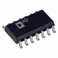
IC VIDEO MULTIPLEXER 4X1 14SOIC

AD8184ARZ

Manufacturer Part Number
AD8184ARZ
Description
IC VIDEO MULTIPLEXER 4X1 14SOIC
Manufacturer
Analog Devices Inc
Datasheet

Specifications of AD8184ARZ

Function
Video Multiplexer
Circuit
1 x 4:1
On-state Resistance
33 Ohm
Voltage Supply Source
Dual Supply
Voltage - Supply, Single/dual (±)
±4 V ~ 6 V
Current - Supply
2.1mA
Operating Temperature
-40°C ~ 85°C
Mounting Type
Surface Mount
Package / Case
14-SOIC (0.154", 3.90mm Width)
Multiplexer Configuration
4
Bandwidth
700MHz
Cross Talk
-95dB
Supply Voltage Range
± 4V To ± 6V
Operating Temperature Range
-40°C To +85°C
Tv / Video Case Style
SOIC
No. Of Pins
14
Lead Free Status / RoHS Status
Lead free / RoHS Compliant

Available stocks

Company
Part Number
Manufacturer
Quantity
Price
Part Number:
AD8184ARZ
Manufacturer:
ADI
Quantity:
455
Part Number:
AD8184ARZ
Manufacturer:
AD
Quantity:
3 048
Part Number:
AD8184ARZ
Manufacturer:
ADI/亚德诺
Quantity:
20 000
Company:
Part Number:
AD8184ARZ
Quantity:
500
Part Number:
AD8184ARZ-REEL
Manufacturer:
RENESAS
Quantity:
831
Part Number:
AD8184ARZ-REEL
Manufacturer:
ADI/亚德诺
Quantity:
20 000
Part Number:
AD8184ARZ-REEL7
Manufacturer:
NXP
Quantity:
6 696
Part Number:
AD8184ARZ-REEL7
Manufacturer:
ADI/亚德诺
Quantity:
20 000
a
PRODUCT DESCRIPTION
The AD8184 is a high speed 4-to-1 multiplexer. It offers –3 dB
signal bandwidth of 700 MHz along with a slew rate of 750 V/ s.
With 95 dB of crosstalk and 115 dB isolation, it is useful in
many high speed applications. The differential gain and differ-
ential phase error of 0.01% and 0.01 , along with 0.1 dB flatness
of 75 MHz, make AD8184 ideal for professional video multi-
plexing. It offers 10 ns switching time, making it an excellent
choice for pixel switching (picture-in-picture) while consuming
less than 4.5 mA on 5 V supply voltage.
The AD8184 offers a high speed disable feature allowing the
output to be put into a high impedance state. This allows mul-
tiple outputs to be connected together for cascading stages while
the “OFF” channels do not load the output bus. It operates on
voltage supplies of 5 V and is offered in 14-lead PDIP and
SOIC packages.
*All trademarks are the property of their respective holders.
REV. 0
Information furnished by Analog Devices is believed to be accurate and
reliable. However, no responsibility is assumed by Analog Devices for its
use, nor for any infringements of patents or other rights of third parties
which may result from its use. No license is granted by implication or
otherwise under any patent or patent rights of Analog Devices.
FEATURES
Single and Dual 2-to-1 Also Available (AD8180 and AD8182)
Fully Buffered Inputs and Outputs
Fast Channel Switching: 10 ns
High Speed
Excellent Video Specifications (R
Low Power: 4.4 mA
Low Glitch: < 25 mV
Low All-Hostile Crosstalk of –95 dB @ 5 MHz
High “OFF” Isolation of –115 dB @ 5 MHz
Low Cost
Fast Output Disable Feature for Connecting Multiple Devices
APPLICATIONS
Pin Compatible with HA4314* and GX4314*
Video Switchers and Routers
Pixel Switching for “Picture-In-Picture”
Switching in LCD and Plasma Displays
> 700 MHz Bandwidth (–3 dB)
> 750 V/ s Slew Rate
Fast Settling Time of 15 ns to 0.1%
Gain Flatness of 0.1 dB of 75 MHz
0.01% Differential Gain Error, R
0.01 Differential Phase Error, R
L
L
L
> 2 k )
= 10 k
= 10 k
One Technology Way, P.O. Box 9106, Norwood, MA 02062-9106, U.S.A.
Tel: 617/329-4700
Fax: 617/326-8703
Figure 1. Small Signal Frequency Response
–1
–2
–3
–4
–5
5
4
3
2
1
0
1M
V
R
ENABLE
0
0
0
0
1
IN
L
FUNCTIONAL BLOCK DIAGRAM
= 5k
= 50mVrms
4-to-1 Video Multiplexer
GND
GND
GND
IN0
IN1
IN2
IN3
World Wide Web Site: http://www.analog.com
Table I. Truth Table
10M
1
2
3
4
5
6
7
NC = NO CONNECT
FREQUENCY – Hz
A1
0
0
1
1
X
+1
+1
+1
+1
DECODER
AD8184
700 MHz, 5 mA
A0
0
1
0
1
X
100M
© Analog Devices, Inc., 1997
14
13
12
11
10
9
8
+V
A0
A1
ENABLE
OUT
NC
–V
S
S
OUTPUT
IN0
IN1
IN2
IN3
High Z
AD8184
1G

Related parts for AD8184ARZ

AD8184ARZ Summary of contents

Page 1

FEATURES Single and Dual 2-to-1 Also Available (AD8180 and AD8182) Fully Buffered Inputs and Outputs Fast Channel Switching High Speed > 700 MHz Bandwidth (–3 dB) > 750 V/ s Slew Rate Fast Settling Time of 15 ...

Page 2

AD8184–SPECIFICATIONS Parameter SWITCHING CHARACTERISTICS 1 Channel Switching Time 50% Logic to 10% Output Settling 50% Logic to 90% Output Settling 50% Logic to 99.9% Output Settling 2 ENABLE to Channel ON Time 50% Logic to 90% Output Settling 2 ENABLE ...

Page 3

NOTES 1 ENABLE pin is grounded. IN0 and IN2 = +1 V dc, IN1 and IN3 = – driven with pulse grounded. Measure transition time from 50% of ...

Page 4

AD8184–Typical Performance Curves DUT OUT 500mV/DIV A0 PULSE OUTPUT –1V 5ns/DIV Figure 3 Channel Switching Characteristics PULSE +1V DUT OUT 800mV/DIV –1V +1V – OFF ON 10ns/DIV Figure 4. Enable and ...

Page 5

OUTPUT @ 50mV OUTPUT @ 100mV 50mV/DIV INPUT 5ns/DIV Figure 9. Small Signal Transient Response + – OUTPUT = 2V 2V/DIV + – OUTPUT = 1V INPUT 10ns/DIV Figure 10. Large Signal Transient Response 0.05 0.04 0.03 0.02 0.01 0.00 ...

Page 6

AD8184–Typical Performance Curves p-p OUT – –20 –30 –40 –50 –60 2ND HARMONIC –70 –80 3RD HARMONIC –90 –100 100k 1M FREQUENCY – Hz Figure 15. Harmonic Distortion vs. Frequency 100M 10M ...

Page 7

THEORY OF OPERATION The AD8184 video multiplexer is designed for fast switching (10 ns) and wide bandwidth (> 700 MHz). This performance is attained with low power dissipation (4.4 mA, enabled) through the use of proprietary circuit techniques and a ...

Page 8

AD8184 Chip capacitors should be used for supply bypassing. One end of the capacitor should be connected to the ground plane and the other within 1/4 inch of each power pin. An additional large (4.7 F–10 F) tantalum capacitor should ...

Page 9

Color Document Scanner Figure 23 shows a block diagram of a Color Document Scanner. Charge Coupled Devices (CCDs) find widespread use in scan- ner applications. A monochrome CCD delivers a serial stream of voltages levels, each level being proportional to ...

Page 10

AD8184 IN0 R4 49.9 IN1 R3 49.9 IN2 R2 49.9 IN3 R1 49.9 EVALUATION BOARD An evaluation board is available for the AD8184. It has been carefully laid out and tested to demonstrate the specified high speed performance of the ...

Page 11

Figure 26. Component Side Silkscreen Figure 27. Board Layout (Component Side) REV. 0 Figure 28. Solder Side Silkscreen Figure 29. Board Layout (Solder Side) –11– AD8184 ...

Page 12

AD8184 0.210 (5.33) 0.160 (4.06) 0.115 (2.93) OUTLINE DIMENSIONS Dimensions shown in inches and (mm). 14-Lead Plastic DIP (N-14) 0.795 (20.19) 0.725 (18.42 0.280 (7.11) 0.240 (6.10) 0.325 (8.25 0.300 (7.62) 0.060 (1.52) PIN 1 0.015 ...

Related keywords