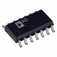
AD8184ARZ Analog Devices Inc, AD8184ARZ Datasheet - Page 7

AD8184ARZ
Manufacturer Part Number
AD8184ARZ
Description
IC VIDEO MULTIPLEXER 4X1 14SOIC
Manufacturer
Analog Devices Inc
Datasheet
1.AD8184ARZ.pdf
(12 pages)
Specifications of AD8184ARZ
Function
Video Multiplexer
Circuit
1 x 4:1
On-state Resistance
33 Ohm
Voltage Supply Source
Dual Supply
Voltage - Supply, Single/dual (±)
±4 V ~ 6 V
Current - Supply
2.1mA
Operating Temperature
-40°C ~ 85°C
Mounting Type
Surface Mount
Package / Case
14-SOIC (0.154", 3.90mm Width)
Multiplexer Configuration
4
Bandwidth
700MHz
Cross Talk
-95dB
Supply Voltage Range
± 4V To ± 6V
Operating Temperature Range
-40°C To +85°C
Tv / Video Case Style
SOIC
No. Of Pins
14
Lead Free Status / RoHS Status
Lead free / RoHS Compliant
Available stocks
Company
Part Number
Manufacturer
Quantity
Price
Company:
Part Number:
AD8184ARZ
Manufacturer:
ADI
Quantity:
455
Part Number:
AD8184ARZ
Manufacturer:
ADI/亚德诺
Quantity:
20 000
Company:
Part Number:
AD8184ARZ-REEL
Manufacturer:
RENESAS
Quantity:
831
Part Number:
AD8184ARZ-REEL
Manufacturer:
ADI/亚德诺
Quantity:
20 000
Company:
Part Number:
AD8184ARZ-REEL7
Manufacturer:
NXP
Quantity:
6 696
Part Number:
AD8184ARZ-REEL7
Manufacturer:
ADI/亚德诺
Quantity:
20 000
THEORY OF OPERATION
The AD8184 video multiplexer is designed for fast switching
(10 ns) and wide bandwidth (> 700 MHz). This performance is
attained with low power dissipation (4.4 mA, enabled) through
the use of proprietary circuit techniques and a dielectrically-
isolated complementary bipolar process. This device has a fast
disable function that allows the outputs of several muxes to be
wired in parallel to form a larger mux with little degradation in
switching time. The low disabled output capacitance (3.2 pF)
helps to preserve the system bandwidth in larger matrices. Un-
like earlier CMOS switches, the switched open-loop buffer ar-
chitecture of the AD8184 provides a unidirectional signal path
with minimal switching glitches and constant, low input capaci-
tance. Since the input impedance of these muxes is nearly inde-
pendent of the load impedance and the state of the mux, the
frequency response of the ON channels in a large switch matrix
is not affected by fanout.
Figure 21 shows a block diagram and simplified schematic of the
AD8184, which contains four switched buffers (S0–S3) that
share a common output. The decoder logic translates TTL-
compatible logic inputs (A0, A1 and ENABLE) to internal, dif-
ferential ECL levels for fast, low-glitch switching. The A0 (LSB)
and A1 (MSB) control inputs constitute a two-bit binary word
that determines which of the four buffers is enabled, unless the
ENABLE input is HIGH, in which case all buffers are disabled
and the output is switched to a high impedance state.
Each open-loop buffer is implemented as a complementary
emitter follower that provides high input impedance, symmetric
slew rate and load drive, and high output-to-input isolation due
to its
switched current sources that allow the buffer to turn on quickly.
Dedicated flatness circuits, combined with the open-loop archi-
tecture of the AD8184, keep peaking low (typically < 0.5 dB)
when driving high capacitive loads, without the need for external
REV. 0
2
current gain. The selected buffer is biased ON by fast
Figure 21. Block Diagram and Simplified Schematic of the AD8184 Multiplexer
GND
GND
GND
IN0
IN1
IN2
IN3
1
2
3
4
5
6
7
S0
S1
S2
S3
I1
Q1
I1
Q1
I1
Q1
I1
Q1
I2
I2
I2
I2
Q2
Q2
Q2
Q2
Q3
Q4
Q3
Q4
Q3
Q4
Q4
Q3
NC = NO CONNECT
–7–
AD8184
series resistors at the input or output. If better flatness response
is desired, an input series resistance (R
Figure 19), although this will increase crosstalk. The dc gain of
the AD8184 is almost independent of load for R
heavier loads, the dc gain is approximately that of the voltage
divider formed by the output impedance of the mux (typically
28
High speed disable clamp circuits (not shown) at the bases of
Q3 and Q4 allow the buffers to turn off quickly and cleanly
without dissipating much power once off. Moreover, these
clamps shunt displacement currents flowing through the junc-
tion capacitances of Q1 and Q2 away from the bases of Q3 and
Q4 and to ac ground through low impedances. The two-pole
high-pass frequency response of the T switch formed by these
clamps is a significant improvement over the one-pole high pass
response of a simple series CMOS switch. As a result, board
and package parasitics, especially stray capacitance between
inputs and outputs, may limit the achievable crosstalk and off
isolation.
LAYOUT CONSIDERATIONS:
Realizing the high speed performance attainable with the
AD8184 requires careful attention to board layout and compo-
nent selection. Proper RF design techniques and low parasitic
component selection are mandatory.
Wire wrap boards, prototype boards and sockets are not recom-
mended because of their high parasitic inductance and capaci-
tance. Instead, surface-mount components should be directly
soldered to a printed circuit board (PCB). The PCB should
have a ground plane covering all unused portions of the compo-
nent side of the board to provide a low impedance ground path.
To reduce stray capacitance the ground plane should be removed
from the area near input and output pins.
and R
L
).
14
13
11
10
12
8
9
V
A0
A1
OUT
NC
V
CC
EE
S
) may be used (refer to
AD8184
L
> 10 k . For


