DG419CJ+ Maxim Integrated Products, DG419CJ+ Datasheet
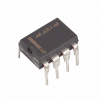
IC SWITCH SPDT 8DIP

DG419CJ+

Manufacturer Part Number
DG419CJ+
Description
IC SWITCH SPDT 8DIP
Manufacturer
Maxim Integrated Products
Type
Analog Switchr
Datasheet

Specifications of DG419CJ+

Function
Switch
Circuit
1 x SPDT
On-state Resistance
35 Ohm
Voltage Supply Source
Single, Dual Supply
Voltage - Supply, Single/dual (±)
10 V ~ 30 V, ±4.5 V ~ 20 V
Operating Temperature
0°C ~ 70°C
Mounting Type
Through Hole
Package / Case
8-DIP (0.300", 7.62mm)
Number Of Switches
Dual
Switch Configuration
SPDT
On Resistance (max)
35 Ohms
On Time (max)
175 ns
Off Time (max)
145 ns
Off Isolation (typ)
68 dB
Supply Voltage (max)
+/- 20 V
Supply Voltage (min)
+/- 4.5 V
Supply Current
- 0.0001 uA
Maximum Power Dissipation
727 mW
Maximum Operating Temperature
+ 70 C
Mounting Style
Through Hole
Description/function
Analog Switch
Input Level
CMOS, TTL
Minimum Operating Temperature
0 C
Off State Leakage Current (max)
5 nA
Package
8PDIP N
Maximum On Resistance
100@10.8V Ohm
Maximum Propagation Delay Bus To Bus
175@±15V ns
Maximum High Level Output Current
30 mA
Switch Architecture
SPDT
Power Supply Type
Single|Dual
Lead Free Status / RoHS Status
Lead free / RoHS Compliant
Maxim’s redesigned DG417/DG418/DG419 precision,
CMOS, monolithic analog switches now feature guar-
anteed on-resistance matching (3Ω max) between
switches and guaranteed on-resistance flatness over
the signal range (4Ω max). These switches conduct
equally well in either direction and guarantee low
charge injection, low power consumption, and an ESD
tolerance of 2000V minimum per Method 3015.7. The
new design offers low off-leakage current over temper-
ature (less than 5nA at +85°C).
The DG417/DG418 are single-pole/single-throw (SPST)
switches. The DG417 is normally closed, and the
DG418 is normally open. The DG419 is single-
pole/double-throw (SPDT) with one normally closed
switch and one normally open switch. Switching times
are less than 175ns max for t
max for t
supply, or bipolar ±4.5V to ±20V supplies. The
improved DG417/DG418/DG419 are fabricated with a
44V silicon-gate process.
________________________Applications
19-0114; Rev 2; 12/96
For free samples & the latest literature: http://www.maxim-ic.com, or phone 1-800-998-8800
_____________________Pin Configurations/Functional Diagrams/Truth Tables
_______________General Description
TOP VIEW
N.C. = NO INTERNAL CONNECTION
Sample-and-Hold Circuits
Test Equipment
Modems
Guidance and Control Systems
Audio Signal Routing
OFF
N.C.
GND
. Operation is from a single +10V to +30V
V+
S
1
2
3
4
________________________________________________________________ Maxim Integrated Products
LOGIC
1
0
Improved, SPST/SPDT Analog Switches
DIP/SO
DG417
DG417
SWITCH
OFF
ON
ON
Communications Systems
Battery-Operated Systems
Fax Machines
PBX, PABX
Military Radios
8
7
6
5
and less than 145ns
D
V-
IN
VL
N.C.
GND
SWITCHES SHOWN FOR LOGIC "0" INPUT
V+
S
1
2
3
4
LOGIC
0
1
DIP/SO
DG418
DG418
Ordering Information continued at end of data sheet.
* Contact factory for dice specifications.
SWITCH
______________________New Features
__________________Existing Features
OFF
______________Ordering Information
DG417CJ
DG417CY
DG417C/D
DG417DJ
DG417DY
ON
Plug-In Upgrades for Industry-Standard
DG417/DG418/DG419
Improved R
(3Ω max, DG419 only)
Guaranteed R
Improved Charge Injection (10pC max)
Improved Off-Leakage Current Over Temperature
(<5nA at +85°C)
Withstand Electrostatic Discharge (2000V min)
per Method 3015.7
Low R
Single-Supply Operation +10V to +30V
Bipolar-Supply Operation ±4.5V to ±20V
Low Power Consumption (35µW max)
Rail-to-Rail Signal Handling
TTL/CMOS-Logic Compatible
PART
8
7
6
5
D
V-
IN
VL
DS(ON)
DS(ON)
GND
FLAT(ON)
(35Ω max)
S1
V+
D
-40°C to +85°C
-40°C to +85°C
TEMP. RANGE
LOGIC
1
0
0°C to +70°C
0°C to +70°C
0°C to +70°C
1
2
3
4
Match Between Channels
Over Signal Range (4Ω max)
DIP/SO
DG419
SWITCH 1
DG419
OFF
ON
SWITCH 2
8 Plastic DIP
8 SO
Dice*
8 Plastic DIP
8 SO
8
7
6
5
PIN-PACKAGE
OFF
ON
S2
V-
IN
VL
1

Related parts for DG419CJ+

DG419CJ+ Summary of contents

Page 1

... DIP/SO DG417 LOGIC SWITCH OFF N. INTERNAL CONNECTION ________________________________________________________________ Maxim Integrated Products For free samples & the latest literature: http://www.maxim-ic.com, or phone 1-800-998-8800 ______________________New Features Plug-In Upgrades for Industry-Standard DG417/DG418/DG419 Improved R (3Ω max, DG419 only) Guaranteed R Improved Charge Injection (10pC max) Improved Off-Leakage Current Over Temperature (< ...

Page 2

Improved, SPST/SPDT Analog Switches ABSOLUTE MAXIMUM RATINGS Voltage Referenced .......................................................................................44V GND....................................................................................25V VL ..................................................(GND - 0.3V) to (V+ + 0.3V) Digital Inputs (Note 1) .........(V- - 2V) to (V+ + 2V) or 30mA S D ...

Page 3

Improved, SPST/SPDT Analog Switches ELECTRICAL CHARACTERISTICS—Dual Supplies (continued) (V+ = +15V -15V 5V, GND = 0V PARAMETER SYMBOL LOGIC INPUT Logic Input Current with I INH Input Voltage High Logic Input Current with I ...

Page 4

Improved, SPST/SPDT Analog Switches ELECTRICAL CHARACTERISTICS—Single Supply (V+ = +12V 0V 5V, GND = 0V, V PARAMETER SYMBOL SWITCH Analog Signal Range V ANALOG Drain-Source On-Resistance R DS(ON) DYNAMIC Turn-On Time t ON Turn-Off Time t ...

Page 5

Improved, SPST/SPDT Analog Switches __________________________________________Typical Operating Characteristics (T = +25°C, unless otherwise noted.) A ON-RESISTANCE vs. V AND D POWER-SUPPLY VOLTAGE 5V - 10V -10V C: ...

Page 6

Improved, SPST/SPDT Analog Switches ______________________________________________________________Pin Description PIN NAME DG417 DG418 DG419 1 — — S — 1 — S — — — N. GND ...

Page 7

Improved, SPST/SPDT Analog Switches _____________________________________________________Test Circuits/Timing Diagrams +3V LOGIC 50% INPUT 0V V OUT 0 SWITCH 0V OUTPUT t ON LOGIC INPUT WAVEFORMS INVERTED FOR SWITCHES THAT HAVE THE OPPOSITE LOGIC SENSE. Figure 2. DG417/DG418 Switching Time +3V ...

Page 8

Improved, SPST/SPDT Analog Switches ______________________________________Test Circuits/Timing Diagrams (continued) LOGIC +3V INPUT 50 OUT1 0 OUT 0V SWITCH OUTPUT 1 V OUT2 SWITCH V t OUT D OUTPUT 2 Figure 4. DG419 Break-Before-Make Interval V OUT IN ...

Page 9

Improved, SPST/SPDT Analog Switches ______________________________________Test Circuits/Timing Diagrams (continued) +15V 10nF SIGNAL V+ GENERATOR 0dBm NETWORK ANALYZER GND R L Figure 6. Off-Isolation Rejection Ratio +15V 10nF V+ D CAPACITANCE METER 1MHz GND Figure ...

Page 10

Improved, SPST/SPDT Analog Switches __Ordering Information (continued) PART TEMP. RANGE DG417DK -40°C to +85°C DG417AK -55°C to +125°C DG418CJ 0°C to +70°C DG418CY 0°C to +70°C DG418C/D 0°C to +70°C DG418DJ -40°C to +85°C DG418DY -40°C to +85°C DG418DK -40°C ...

Page 11

Improved, SPST/SPDT Analog Switches ________________________________________________________Package Information ______________________________________________________________________________________ 11 ...

Page 12

... Maxim reserves the right to change the circuitry and specifications without notice at any time __________________Maxim Integrated Products, 120 San Gabriel Drive, Sunnyvale, CA 94086 (408) 737-7600 __________________Maxim Integrated Products, 120 San Gabriel Drive, Sunnyvale, CA 94086 (408) 737-7600 © 1996 Maxim Integrated Products © ...

Related keywords