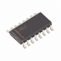
MAX4053ACSE+ Maxim Integrated Products, MAX4053ACSE+ Datasheet

MAX4053ACSE+
Specifications of MAX4053ACSE+
Related parts for MAX4053ACSE+
MAX4053ACSE+ Summary of contents
Page 1
... LOGIC GND 8 9 DIP/SO/QSOP ________________________________________________________________ Maxim Integrated Products For pricing, delivery, and ordering information, please contact Maxim/Dallas Direct! at 1-888-629-4642, or visit Maxim’s website at www.maxim-ic.com. Low-Voltage, CMOS Analog Multiplexers/Switches ____________________________Features ♦ Pin Compatible with Industry-Standard 74HC4051/74HC4052/74HC4053 ♦ Guaranteed On-Resistance: 100Ω with ±5V Supplies ♦ ...
Page 2
Low-Voltage, CMOS Analog Multiplexers/Switches ABSOLUTE MAXIMUM RATINGS Voltages Referenced to GND V+ ........................................................................-0.3V to +17V V-..........................................................................+0.3V to -17V ................................................................-0.3V to +17V Voltage into Any Terminal (Note 1) ..........(V- - 2V) to (V+ + 2V) or 30mA (whichever ...
Page 3
ELECTRICAL CHARACTERISTICS—Dual Supplies (continued) (V+ = +4.5V to +5.5V -4.5V to -5.5V, T PARAMETER SYMBOL COM Off-Leakage I COM(OFF) Current (Note 5) COM On-Leakage I COM(ON) Current (Note 5) _______________________________________________________________________________________ Low-Voltage, CMOS Analog Multiplexers/Switches = ...
Page 4
Low-Voltage, CMOS Analog Multiplexers/Switches ELECTRICAL CHARACTERISTICS—Dual Supplies (continued) (V+ = +4.5V to +5.5V -4.5V to -5.5V, T PARAMETER SYMBOL DIGITAL I/O ADD, INH Input Logic V IH Threshold High ADD, INH Input Logic V IL Threshold Low ADD, ...
Page 5
ELECTRICAL CHARACTERISTICS—Single +5V Supply (V+ = +4.5V to +5.5V 0V MIN PARAMETER SYMBOL ANALOG SWITCH Analog Signal Range COM NO COM–NO On-Resistance Off-Leakage Current I NO(OFF) (Note 5) ...
Page 6
Low-Voltage, CMOS Analog Multiplexers/Switches ELECTRICAL CHARACTERISTICS—Single +5V Supply (continued) (V+ = +4.5V to +5.5V 0V MIN PARAMETER SYMBOL DIGITAL I/O SWITCH DYNAMIC CHARACTERISTICS Turn-On Time (Note Turn-Off Time (Note 6) t ...
Page 7
ELECTRICAL CHARACTERISTICS—Single +3V Supply (V+ = +3.0V to +3.6V 0V MIN PARAMETER SYMBOL ANALOG SWITCH Analog Signal Range COM NO COM–NO On-Resistance Off-Leakage Current I NO(OFF) (Note 5) ...
Page 8
Low-Voltage, CMOS Analog Multiplexers/Switches ELECTRICAL CHARACTERISTICS—Single +3V Supply (continued) (V+ = +3.0V to +3.6V 0V MIN PARAMETER SYMBOL SWITCH DYNAMIC CHARACTERISTICS DIGITAL I/O Turn-On Time (Note Turn-Off Time (Note 6) t ...
Page 9
Operating Characteristics (V+ = +5V -5V, GND = 0V +25°C, unless otherwise noted.) A ON-RESISTANCE vs. V COM (DUAL SUPPLIES) 110 100 90 V± = ± V± = ± ...
Page 10
Low-Voltage, CMOS Analog Multiplexers/Switches ____________________________Typical Operating Characteristics (continued) (V+ = +5V -5V, GND = 0V +25°C, unless otherwise noted.) A FREQUENCY RESPONSE 0 -10 -20 INSERTION LOSS -30 -40 OFF-ISOLATION -50 -60 -70 ON PHASE -80 ...
Page 11
Table 1. Truth Table/Switch Programming ADDRESS BITS INH ADDC* ADDB Don’t ...
Page 12
Low-Voltage, CMOS Analog Multiplexers/Switches V+ and GND power the internal logic and logic-level translators, and set both the input and output logic lim- its. The logic-level translators convert the logic levels into switched V+ and V- signals to drive the ...
Page 13
Circuits/Timing Diagrams V+ V ADD V+ ADDC ADDB NO1–NO6 ADDA MAX4051/A 50Ω INH COM GND ADD V+ ADDA ADDB NO1–NO2 MAX4052/A 50Ω INH COM GND ADD V+ ADD MAX4053/A 50Ω INH ...
Page 14
Low-Voltage, CMOS Analog Multiplexers/Switches V+ V+ ADDC ADDB NO1–NO7 ADDA MAX4051/A V INH INH COM GND V- 50Ω ADDA ADDB NO1–NO3 MAX4052/A V INH INH COM GND V- 50Ω ADD MAX4053/A V INH INH ...
Page 15
V+ V ADD V+ ADDC NO0–N07 ADDB ADDA MAX4051/A 50Ω INH COM GND V- 300Ω ADD V+ NO, NC ADD MAX4053/A 50Ω INH COM GND V- 300Ω FOR SINGLE-SUPPLY OPERATION. REPEAT TEST FOR ...
Page 16
Low-Voltage, CMOS Analog Multiplexers/Switches ADDC CHANNEL ADDB MAX4051/A SELECT ADDA MAX4052/A MAX4053/A INH GND MEASUREMENTS ARE STANDARDIZED AGAINST SHORT AT SOCKET TERMINALS. OFF-ISOLATION IS MEASURED BETWEEN COM AND "OFF" NO TERMINAL ON EACH SWITCH. ON-LOSS IS MEASURED BETWEEN COM AND ...
Page 17
Information (continued) PART TEMP RANGE MAX4051AEPE -40°C to +85°C MAX4051AESE -40°C to +85°C MAX4051AEEE -40°C to +85°C MAX4051AMJE -55°C to +125°C MAX4051CPE 0°C to +70°C MAX4051CSE 0°C to +70°C MAX4051CEE 0°C to +70°C MAX4051C/D 0°C to +70°C MAX4051EPE -40°C ...
Page 18
Low-Voltage, CMOS Analog Multiplexers/Switches (The package drawing(s) in this data sheet may not reflect the most current specifications. For the latest package outline information www.maxim-ic.com/packages.) 18 ______________________________________________________________________________________ Package Information ...
Page 19
... Maxim cannot assume responsibility for use of any circuitry other than circuitry entirely embodied in a Maxim product. No circuit patent licenses are implied. Maxim reserves the right to change the circuitry and specifications without notice at any time. Maxim Integrated Products, 120 San Gabriel Drive, Sunnyvale, CA 94086 (408) 737-7600___________________ 19 © 2005 Maxim Integrated Products ...


