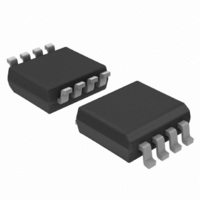
74LVC2G66DC,125 NXP Semiconductors, 74LVC2G66DC,125 Datasheet - Page 5

74LVC2G66DC,125
Manufacturer Part Number
74LVC2G66DC,125
Description
IC SWITCH DUAL SPST 8VSSOP
Manufacturer
NXP Semiconductors
Series
74LVCr
Type
Analog Switchr
Datasheet
1.74LVC2G66GM125.pdf
(26 pages)
Specifications of 74LVC2G66DC,125
Package / Case
8-VFSOP (0.091", 2.3mm Width)
Function
Switch
Circuit
2 x SPST - NO
On-state Resistance
6 Ohm
Voltage Supply Source
Single Supply
Voltage - Supply, Single/dual (±)
1.65 V ~ 5.5 V
Current - Supply
0.1µA
Operating Temperature
-40°C ~ 125°C
Mounting Type
Surface Mount
Switch Configuration
SPST
On Resistance (max)
34 Ohm (Typ) @ 1.95 V
On Time (max)
4.6 ns (Typ) @ 1.95 V
Off Time (max)
3.8 ns (Typ) @ 1.95 V
Supply Voltage (max)
5.5 V
Supply Voltage (min)
1.65 V
Maximum Power Dissipation
250 mW
Maximum Operating Temperature
+ 125 C
Mounting Style
SMD/SMT
Minimum Operating Temperature
- 40 C
Switch Current (typ)
0.0001 mA @ 5.5 V
Package
8VSSOP
Maximum On Resistance
195@1.95V Ohm
Maximum Propagation Delay Bus To Bus
0.8(Typ)@1.95V|0.4(Typ)@2.7V|0.3(Typ)@3.6V|0.2(Typ)@5.5V ns
Maximum Low Level Output Current
50 mA
Maximum Turn-off Time
3.8(Typ)@1.95V ns
Maximum Turn-on Time
4.6(Typ)@1.95V ns
Switch Architecture
SPST
Power Supply Type
Single
Lead Free Status / RoHS Status
Lead free / RoHS Compliant
Lead Free Status / RoHS Status
Lead free / RoHS Compliant, Lead free / RoHS Compliant
Other names
74LVC2G66DC-G
74LVC2G66DC-G
935274429125
74LVC2G66DC-G
935274429125
NXP Semiconductors
9. Recommended operating conditions
Table 6.
[1]
[2]
[3]
10. Static characteristics
Table 7.
At recommended operating conditions; voltages are referenced to GND (ground = 0 V).
74LVC2G66
Product data sheet
Symbol
V
V
V
T
Δt/ΔV
Symbol Parameter
V
V
I
I
I
I
ΔI
I
S(OFF)
S(ON)
CC
amb
CC
I
SW
IH
IL
CC
To avoid sinking GND current from terminal nZ when switch current flows in terminal nY, the voltage drop across the bidirectional switch
must not exceed 0.4 V. If the switch current flows into terminal nZ, no GND current will flow from terminal nY. In this case, there is no
limit for the voltage drop across the switch.
For overvoltage tolerant switch voltage capability, refer to 74LVCV2G66.
Applies to control signal levels.
HIGH-level
input voltage
LOW-level
input voltage
input leakage
current
OFF-state
leakage
current
ON-state
leakage
current
supply current
additional
supply current
Operating conditions
Static characteristics
Parameter
supply voltage
input voltage
switch voltage
ambient temperature
input transition rise and fall rate
Conditions
V
V
V
V
V
V
V
V
pin nE; V
V
V
V
V
V
pin nE; V
V
V
V
CC
CC
CC
CC
CC
CC
CC
CC
CC
CC
I
SW
CC
SW
CC
CC
= 5.5 V or GND;
= 1.65 V to 1.95 V
= 2.3 V to 2.7 V
= 2.7 V to 3.6 V
= 4.5 V to 5.5 V
= 1.65 V to 1.95 V
= 2.3 V to 2.7 V
= 2.7 V to 3.6 V
= 4.5 V to 5.5 V
= 0 V to 5.5 V
= 5.5 V; see
= 1.65 V to 5.5 V
= 5.5 V
= GND or V
= GND or V
= 5.5 V; see
I
I
= 5.5 V or GND;
= V
CC
All information provided in this document is subject to legal disclaimers.
CC
CC
− 0.6 V;
Figure 8
Figure 9
;
;
Conditions
V
V
Rev. 5 — 16 June 2010
CC
CC
= 1.65 V to 2.7 V
= 2.7 V to 5.5 V
[2]
[2]
[2]
[2]
[2]
0.65 × V
0.7 × V
Min
1.7
2.0
-
-
-
-
-
-
-
-
-
−40 °C to +85 °C
CC
CC
Typ
±0.1
±0.1
±0.1
0.1
5
-
-
-
-
-
-
-
-
[1]
0.35 × V
0.3 × V
Max
500
0.7
0.8
±5
±5
±5
10
-
-
-
-
[1][2]
CC
CC
[3]
[3]
Min
1.65
0
0
−40
-
-
0.65 × V
0.7 × V
−40 °C to +125 °C
74LVC2G66
Min
1.7
2.0
-
-
-
-
-
-
-
-
-
CC
CC
© NXP B.V. 2010. All rights reserved.
Max
5.5
5.5
V
+125
20
10
Bilateral switch
CC
0.35 × V
0.3 × V
±100
±200
±200
5000
Max
200
0.7
0.8
-
-
-
-
CC
CC
Unit
V
V
V
°C
ns/V
ns/V
5 of 26
Unit
V
V
V
V
V
V
V
V
μA
μA
μA
μA
μA


