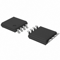
74LVC2G53DP,125 NXP Semiconductors, 74LVC2G53DP,125 Datasheet - Page 11

74LVC2G53DP,125
Manufacturer Part Number
74LVC2G53DP,125
Description
IC MUX/DEMUX 2X1 8TSSOP
Manufacturer
NXP Semiconductors
Series
74LVCr
Type
Analog Multiplexerr
Datasheet
1.74LVC2G53DC125.pdf
(28 pages)
Specifications of 74LVC2G53DP,125
Package / Case
8-TSSOP
Function
Multiplexer/Demultiplexer
Circuit
1 x 2:1
On-state Resistance
6 Ohm
Voltage Supply Source
Single Supply
Voltage - Supply, Single/dual (±)
1.65 V ~ 5.5 V
Current - Supply
0.1µA
Operating Temperature
-40°C ~ 125°C
Mounting Type
Surface Mount
Number Of Channels
1 Channel
On Resistance (max)
34 Ohm (Typ) @ 1.95 V
On Time (max)
6.7 ns (Typ) @ 1.95 V
Off Time (max)
6.8 ns (Typ) @ 1.95 V
Supply Voltage (max)
5.5 V
Supply Voltage (min)
1.65 V
Maximum Power Dissipation
250 mW
Maximum Operating Temperature
+ 125 C
Minimum Operating Temperature
- 40 C
Mounting Style
SMD/SMT
Number Of Switches
Single
Switch Current (typ)
0.0001 mA @ 5.5 V
Package
8TSSOP
Maximum On Resistance
195@1.95V Ohm
Maximum Propagation Delay Bus To Bus
2.5@1.95V@-40C to 125C|1.5@2.7V@-40C to 125C|1@3.6V@-40C to 125C|0.8@5.5V@-40C to 125C ns
Maximum Low Level Output Current
50 mA
Multiplexer Architecture
2:1
Maximum Turn-off Time
6.8(Typ)@1.95V ns
Maximum Turn-on Time
6.7(Typ)@1.95V ns
Power Supply Type
Single
Lead Free Status / RoHS Status
Lead free / RoHS Compliant
Lead Free Status / RoHS Status
Lead free / RoHS Compliant, Lead free / RoHS Compliant
Other names
74LVC2G53DP-G
74LVC2G53DP-G
935280383125
74LVC2G53DP-G
935280383125
NXP Semiconductors
11. Dynamic characteristics
Table 9.
At recommended operating conditions; voltages are referenced to GND (ground = 0 V); for test circuit see
[1]
[2]
[3]
[4]
[5]
74LVC2G53
Product data sheet
Symbol Parameter
t
t
t
pd
en
dis
Typical values are measured at T
t
Propagation delay is the calculated RC time constant of the typical ON resistance of the switch and the specified capacitance when
driven by an ideal voltage source (zero output impedance).
t
t
pd
en
dis
is the same as t
is the same as t
is the same as t
propagation delay Z to Yn or Yn to Z; see
enable time
disable time
Dynamic characteristics
PLH
PZH
PLZ
and t
and t
and t
PHL
PZL
PHZ
Conditions
S to Z or Yn; see
E to Z or Yn; see
S to Z or Yn; see
E to Z or Yn; see
.
.
.
V
V
V
V
V
V
V
V
V
V
V
V
V
V
V
V
V
V
V
V
V
V
V
V
V
amb
CC
CC
CC
CC
CC
CC
CC
CC
CC
CC
CC
CC
CC
CC
CC
CC
CC
CC
CC
CC
CC
CC
CC
CC
CC
= 1.65 V to 1.95 V
= 2.3 V to 2.7 V
= 2.7 V
= 3.0 V to 3.6 V
= 4.5 V to 5.5 V
= 1.65 V to 1.95 V
= 2.3 V to 2.7 V
= 2.7 V
= 3.0 V to 3.6 V
= 4.5 V to 5.5 V
= 1.65 V to 1.95 V
= 2.3 V to 2.7 V
= 2.7 V
= 3.0 V to 3.6 V
= 4.5 V to 5.5 V
= 1.65 V to 1.95 V
= 2.3 V to 2.7 V
= 2.7 V
= 3.0 V to 3.6 V
= 4.5 V to 5.5 V
= 1.65 V to 1.95 V
= 2.3 V to 2.7 V
= 2.7 V
= 3.0 V to 3.6 V
= 4.5 V to 5.5 V
= 25 °C and nominal V
All information provided in this document is subject to legal disclaimers.
Figure 17
Figure 17
Figure 17
Figure 17
Rev. 6 — 27 September 2010
Figure 16
CC
.
[2][3]
[4]
[4]
[5]
[5]
Min
2-channel analog multiplexer/demultiplexer
1.9
1.8
1.3
1.4
1.2
1.0
1.4
1.1
1.0
1.2
2.0
1.3
2.6
1.9
1.9
1.1
2.1
1.4
2.3
1.4
-
-
-
-
-
−40 °C to +85 °C
Typ
6.7
4.1
4.0
3.4
2.6
4.0
2.5
2.6
2.2
1.7
6.8
3.7
4.9
4.0
2.9
5.6
3.2
4.0
3.7
2.9
-
-
-
-
-
[1]
Max
10.3
10.0
1.2
0.8
0.6
6.4
5.5
5.0
3.8
7.3
4.4
3.9
3.8
2.6
6.1
6.2
5.4
3.8
8.6
4.8
5.2
5.0
3.8
1.0
2
74LVC2G53
−40 °C to +125 °C Unit
Min
2.6
1.9
1.8
1.8
1.3
1.9
1.4
1.1
1.2
1.0
2.1
1.4
1.4
1.1
1.0
2.3
1.2
1.4
2.0
1.3
-
-
-
-
-
© NXP B.V. 2010. All rights reserved.
Figure
Max
1.25
12.9
12.5
11.0
2.5
1.5
1.0
0.8
8.0
7.0
6.3
4.8
9.2
5.5
4.9
4.8
3.3
7.7
7.8
6.8
4.8
6.0
6.5
6.3
4.8
18.
11 of 28
ns
ns
ns
ns
ns
ns
ns
ns
ns
ns
ns
ns
ns
ns
ns
ns
ns
ns
ns
ns
ns
ns
ns
ns
ns


