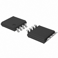
74LVC2G53DP,125 NXP Semiconductors, 74LVC2G53DP,125 Datasheet - Page 8

74LVC2G53DP,125
Manufacturer Part Number
74LVC2G53DP,125
Description
IC MUX/DEMUX 2X1 8TSSOP
Manufacturer
NXP Semiconductors
Series
74LVCr
Type
Analog Multiplexerr
Datasheet
1.74LVC2G53DC125.pdf
(28 pages)
Specifications of 74LVC2G53DP,125
Package / Case
8-TSSOP
Function
Multiplexer/Demultiplexer
Circuit
1 x 2:1
On-state Resistance
6 Ohm
Voltage Supply Source
Single Supply
Voltage - Supply, Single/dual (±)
1.65 V ~ 5.5 V
Current - Supply
0.1µA
Operating Temperature
-40°C ~ 125°C
Mounting Type
Surface Mount
Number Of Channels
1 Channel
On Resistance (max)
34 Ohm (Typ) @ 1.95 V
On Time (max)
6.7 ns (Typ) @ 1.95 V
Off Time (max)
6.8 ns (Typ) @ 1.95 V
Supply Voltage (max)
5.5 V
Supply Voltage (min)
1.65 V
Maximum Power Dissipation
250 mW
Maximum Operating Temperature
+ 125 C
Minimum Operating Temperature
- 40 C
Mounting Style
SMD/SMT
Number Of Switches
Single
Switch Current (typ)
0.0001 mA @ 5.5 V
Package
8TSSOP
Maximum On Resistance
195@1.95V Ohm
Maximum Propagation Delay Bus To Bus
2.5@1.95V@-40C to 125C|1.5@2.7V@-40C to 125C|1@3.6V@-40C to 125C|0.8@5.5V@-40C to 125C ns
Maximum Low Level Output Current
50 mA
Multiplexer Architecture
2:1
Maximum Turn-off Time
6.8(Typ)@1.95V ns
Maximum Turn-on Time
6.7(Typ)@1.95V ns
Power Supply Type
Single
Lead Free Status / RoHS Status
Lead free / RoHS Compliant
Lead Free Status / RoHS Status
Lead free / RoHS Compliant, Lead free / RoHS Compliant
Other names
74LVC2G53DP-G
74LVC2G53DP-G
935280383125
74LVC2G53DP-G
935280383125
NXP Semiconductors
Table 8.
At recommended operating conditions; voltages are referenced to GND (ground 0 V); for graphs see
[1]
[2]
74LVC2G53
Product data sheet
Symbol
R
R
Fig 9.
ON(rail)
ON(flat)
Typical values are measured at T
Flatness is defined as the difference between the maximum and minimum value of ON resistance measured at identical V
temperature.
R
Test circuit for measuring ON resistance
Parameter
ON resistance (rail)
ON resistance
(flatness)
ON
ON resistance
= V
10.3 ON resistance test circuit and graphs
SW
/ I
SW
.
…continued
V
IL
or V
amb
Conditions
V
V
V
V
IH
IL
I
I
I
I
V
I
I
I
I
I
V
I
I
I
I
I
V
I
I
I
I
= 25 °C and nominal V
= GND; see
= V
= GND to V
SW
SW
SW
SW
SW
SW
SW
SW
SW
SW
SW
SW
SW
SW
SW
CC
CC
CC
CC
= 4 mA;
= 8 mA; V
= 12 mA; V
= 24 mA; V
= 32 mA; V
= 4 mA;
= 8 mA; V
= 12 mA; V
= 24 mA; V
= 32 mA; V
= 4 mA;
= 8 mA; V
= 12 mA; V
= 24 mA; V
= 32 mA; V
V I
= 1.65 V to 1.95 V
= 1.65 V to 1.95 V
= 1.65 V to 1.95 V
All information provided in this document is subject to legal disclaimers.
; see
S
Z
Rev. 6 — 27 September 2010
Figure 9
CC
Figure 9
E
CC
CC
CC
V
CC
CC
CC
CC
CC
CC
CC
CC
CC
CC
= 2.3 V to 2.7 V
= 2.3 V to 2.7 V
= 2.3 V to 2.7 V
= 2.7 V
= 3 V to 3.6 V
= 4.5 V to 5.5 V
= 2.7 V
= 3 V to 3.6 V
= 4.5 V to 5.5 V
= 2.7 V
= 3 V to 3.6 V
= 4.5 V to 5.5 V
GND
Y0
Y1
CC
.
V SW
1
2
switch
2-channel analog multiplexer/demultiplexer
[2]
I SW
switch
Min
−40 °C to +85 °C
1
2
-
-
-
-
-
-
-
-
-
-
-
-
-
-
-
V
Typ
V
S
10.4
26.0
IH
IL
8.2
7.1
6.9
6.5
5.8
7.6
7.0
6.1
4.9
5.0
3.5
2.0
1.5
001aad392
[1]
V
V
E
IL
IL
Max
18
16
14
12
10
30
20
18
15
10
-
-
-
-
-
74LVC2G53
−40 °C to +125 °C Unit
Figure 10
Min
-
-
-
-
-
-
-
-
-
-
-
-
-
-
-
© NXP B.V. 2010. All rights reserved.
to
Max
27
24
21
18
15
45
30
27
23
15
CC
-
-
-
-
-
Figure
and
8 of 28
Ω
Ω
Ω
Ω
Ω
Ω
Ω
Ω
Ω
Ω
Ω
Ω
Ω
Ω
Ω
15.


