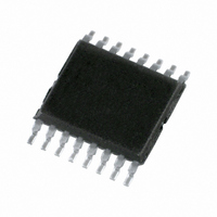
HEF4051BTT,118 NXP Semiconductors, HEF4051BTT,118 Datasheet - Page 13

HEF4051BTT,118
Manufacturer Part Number
HEF4051BTT,118
Description
IC MUX/DEMUX 8X1 16TSSOP
Manufacturer
NXP Semiconductors
Series
4000Br
Datasheet
1.HEF4051BT653.pdf
(23 pages)
Specifications of HEF4051BTT,118
Package / Case
16-TSSOP (0.173", 4.40mm Width)
Function
Multiplexer/Demultiplexer
Circuit
1 x 8:1
On-state Resistance
175 Ohm
Voltage Supply Source
Single, Dual Supply
Voltage - Supply, Single/dual (±)
3 V ~ 15 V, ±15 V
Current - Supply
80µA
Operating Temperature
-40°C ~ 85°C
Mounting Type
Surface Mount
Number Of Channels
1 Channel
On Resistance (max)
2500 Ohm @ 5 V
On Time (max)
280 ns @ 5 V
Off Time (max)
290 ns @ 5 V
Supply Voltage (max)
15 V
Supply Voltage (min)
3 V
Maximum Operating Temperature
+ 85 C
Minimum Operating Temperature
- 40 C
Mounting Style
SMD/SMT
Number Of Switches
Single
Lead Free Status / RoHS Status
Lead free / RoHS Compliant
Lead Free Status / RoHS Status
Lead free / RoHS Compliant, Lead free / RoHS Compliant
Other names
568-1875-2
935278637118
HEF4051BTT-T
935278637118
HEF4051BTT-T
NXP Semiconductors
Table 11.
V
[1]
Table 12.
P
HEF4051B_9
Product data sheet
Symbol
THD
f
α
V
Xtalk
Symbol
P
(−3dB)
SS
D
Fig 17. Test circuit for measuring total harmonic
iso
ct
D
can be calculated from the formulas shown; V
= V
f
i
is biased at 0.5 V
V
EE
DD
distortion
= 0 V; T
or V
Additional dynamic characteristics
Dynamic power dissipation P
Parameter
dynamic power
dissipation
V
SS
SS
11.2.1 Test circuits
Parameter
total harmonic distortion
−3 dB frequency response
isolation (OFF-state)
crosstalk voltage
crosstalk
11.2 Additional dynamic parameters
amb
DD
S1 to S3
Z
f i
= 25
E
; V
V
I
DD
= 0.5V
°
C.
V
Yn
SS
V
5 V
10 V
15 V
DD
DD
= V
(p-p).
EE
R L
All information provided in this document is subject to legal disclaimers.
Typical formula for P
P
P
P
D
Conditions
see
channel ON; V
f
see
channel ON; V
see
C
V
digital inputs to switch; see
R
E or Sn = V
between switches; see
f
V
D
D
D
i
i
I
I
= 1 kHz
L
L
= 1 MHz; R
= 1000 × f
= 5500 × f
= 15000 × f
= 0.5V
= 0.5V
C L
001aak516
= 5 pF; channel OFF;
= 10 kΩ; C
Figure
Figure
Figure
EE
Rev. 09 — 25 March 2010
= V
D
DD
DD
SS
17; R
18; R
19; f
DD
i
i
(p-p)
(p-p)
L
+ Σ(f
+ Σ(f
i
= 0 V; t
L
+ Σ(f
= 1 kΩ;
I
I
(square-wave)
= 15 pF;
= 0.5V
= 0.5V
i
L
L
= 1 MHz; R
o
o
= 10 kΩ; C
= 1 kΩ; C
o
× C
× C
Fig 18. Test circuit for measuring frequency response
× C
D
r
= t
DD
DD
(μW)
L
L
Figure
) × V
) × V
L
f
) × V
V
(p-p);
(p-p)
≤
DD
Figure
20 ns; T
L
L
8-channel analog multiplexer/demultiplexer
DD
DD
or V
L
= 5 pF;
= 1 kΩ;
DD
= 15 pF;
21;
V
2
2
SS
SS
2
20;
amb
S1 to S3
Z
f i
= 25
V
5 V
10 V
15 V
5 V
10 V
15 V
10 V
10 V
10 V
where:
f
f
C
V
Σ(C
E
i
o
DD
DD
= input frequency in MHz;
L
V
= output frequency in MHz;
DD
= output load capacitance in pF;
L
°
= supply voltage in V;
C.
× f
V
Yn
o
SS
) = sum of the outputs.
[1]
[1]
[1]
[1]
[1]
[1]
[1]
[1]
= V
EE
HEF4051B
Typ
0.25
0.04
0.04
13
40
70
−50
50
−50
© NXP B.V. 2010. All rights reserved.
R L
Max
-
-
-
-
-
-
-
001aak517
C L
-
-
dB
13 of 23
Unit
%
%
%
MHz
MHz
MHz
dB
mV
dB


