ADG749BKSZ-REEL7 Analog Devices Inc, ADG749BKSZ-REEL7 Datasheet
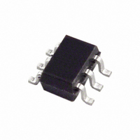
IC SWITCH SPDT SC70-6

ADG749BKSZ-REEL7

Manufacturer Part Number
ADG749BKSZ-REEL7
Description
IC SWITCH SPDT SC70-6
Manufacturer
Analog Devices Inc
Type
Analog Switchr
Datasheet

Specifications of ADG749BKSZ-REEL7

Function
Switch
Circuit
1 x SPDT
On-state Resistance
5 Ohm
Voltage Supply Source
Single Supply
Voltage - Supply, Single/dual (±)
1.8 V ~ 5.5 V
Current - Supply
0.001µA
Operating Temperature
-40°C ~ 85°C
Mounting Type
Surface Mount
Package / Case
6-TSSOP, SC-88, SOT-363
Analog Switch Type
SPDT
No. Of Channels
1
Bandwidth
200MHz
On State Resistance Max
2.5ohm
Turn Off Time
3ns
Turn On Time
7ns
Supply Voltage Range
1.8V To 5.5V
Multiplexer Configuration
Single SPDT
Number Of Inputs
1
Number Of Outputs
2
Number Of Channels
1
Analog Switch On Resistance
12@3VOhm
Analog Switch Turn On Time
10ns
Analog Switch Turn Off Time
4ns
Package Type
SC-70
Power Supply Requirement
Single
Single Supply Voltage (min)
1.8V
Single Supply Voltage (typ)
3/5V
Single Supply Voltage (max)
5.5V
Dual Supply Voltage (min)
Not RequiredV
Dual Supply Voltage (typ)
Not RequiredV
Dual Supply Voltage (max)
Not RequiredV
Power Dissipation
315mW
Supply Current
0.001mA
Mounting
Surface Mount
Pin Count
6
Operating Temp Range
-40C to 125C
Operating Temperature Classification
Automotive
Lead Free Status / RoHS Status
Lead free / RoHS Compliant
Lead Free Status / RoHS Status
Lead free / RoHS Compliant, Lead free / RoHS Compliant
Other names
ADG749BKSZ-REEL7TR

Available stocks

Company
Part Number
Manufacturer
Quantity
Price
Part Number:
ADG749BKSZ-REEL7
Manufacturer:
AD
Quantity:
500
Part Number:
ADG749BKSZ-REEL7
Manufacturer:
NSC
Quantity:
147
Part Number:
ADG749BKSZ-REEL7
Manufacturer:
ADI/亚德诺
Quantity:
20 000
Company:
Part Number:
ADG749BKSZ-REEL7
Quantity:
10 000
FEATURES
1.8 V to 5.5 V single supply
5 Ω (maximum) on resistance
0.75 Ω (typical) on resistance flatness
Automotive temperature range: −40°C to +125°C
–3 dB bandwidth > 200 MHz
Rail-to-rail operation
6-lead SC70 package
Fast switching times
Typical power consumption (< 0.01 μW)
TTL/CMOS compatible
APPLICATIONS
Battery-powered systems
Communication systems
Sample-and-hold systems
Audio signal routing
Video switching
Mechanical reed relay replacement
GENERAL DESCRIPTION
The ADG749 is a monolithic CMOS SPDT switch. This switch
is designed on a submicron process that provides low power
dissipation yet gives high switching speed, low on resistance,
and low leakage currents.
The ADG749 can operate from a single-supply range of 1.8 V to
5.5 V, making it ideal for use in battery-powered instruments
and with the new generation of DACs and ADCs from Analog
Devices, Inc.
Each switch of the ADG749 conducts equally well in both
directions when on. The ADG749 exhibits break-before-make
switching action.
Because of the advanced submicron process, −3 dB bandwidths
of greater than 200 MHz can be achieved.
The ADG749 is available in a 6-lead SC70 package.
Rev. B
Information furnished by Analog Devices is believed to be accurate and reliable. However, no
responsibility is assumed by Analog Devices for its use, nor for any infringements of patents or other
rights of third parties that may result from its use. Specifications subject to change without notice. No
license is granted by implication or otherwise under any patent or patent rights of Analog Devices.
Trademarks and registered trademarks are the property of their respective owners.
t
t
ON
OFF
= 12 ns
= 6 ns
2:1 Mux/SPDT Switch in SC70 Package
One Technology Way, P.O. Box 9106, Norwood, MA 02062-9106, U.S.A.
Tel: 781.329.4700
Fax: 781.461.3113
PRODUCT HIGHLIGHTS
1.
2.
3.
4.
5.
6.
7.
8.
1.8 V to 5.5 V Single-Supply Operation. The ADG749
offers high performance, including low on resistance and
fast switching times, and is fully specified and guaranteed
with 3 V and 5 V supply rails.
Very Low R
at 3 V). At 1.8 V operation, R
temperature range.
Automotive Temperature Range: −40°C to +125°C.
On Resistance Flatness (R
−3 dB Bandwidth > 200 MHz.
Low Power Dissipation. CMOS construction ensures low
power dissipation.
Fast t
Tiny, 6-lead SC70 Package.
CMOS 1.8 V to 5.5 V, 2.5 Ω
ON
FUNCTIONAL BLOCK DIAGRAM
/t
OFF
ON
.
©2005–2009 Analog Devices, Inc. All rights reserved.
(5 Ω Maximum at 5 V and 10 Ω Maximum
S2
S1
IN
SWITCH SHOWN FOR
A LOGIC 1 INPUT
ADG749
Figure 1.
FLAT(ON)
ON
is typically 40 Ω over the
) (0.75 Ω typical).
D
ADG749
www.analog.com

Related parts for ADG749BKSZ-REEL7

ADG749BKSZ-REEL7 Summary of contents

Page 1

FEATURES 1 5.5 V single supply 5 Ω (maximum) on resistance 0.75 Ω (typical) on resistance flatness Automotive temperature range: −40°C to +125°C –3 dB bandwidth > 200 MHz Rail-to-rail operation 6-lead SC70 package Fast switching times t ...

Page 2

ADG749 TABLE OF CONTENTS Features .............................................................................................. 1 Applications ....................................................................................... 1 Functional Block Diagram .............................................................. 1 General Description ......................................................................... 1 Product Highlights ........................................................................... 1 Revision HistoryRevision History .................................................. 2 Specifications ..................................................................................... 3 Absolute Maximum Ratings ............................................................ 5 ESD Caution .................................................................................. 5 ...

Page 3

SPECIFICATIONS ± 10% and GND = −40°C to +125°C unless otherwise stated Table 1. Parameter 25°C ANALOG SWITCH Analog Signal Range On Resistance ( Resistance ...

Page 4

ADG749 ± 10% and GND = −40°C to +125°C unless otherwise stated DD A Table 2. Parameter 25°C ANALOG SWITCH Analog Signal Range On Resistance ( Resistance Match ...

Page 5

ABSOLUTE MAXIMUM RATINGS T = 25°C unless otherwise noted. A Table 3. Parameter Ratings V to GND −0 Analog, Digital Input −0 whichever occurs first Peak Current 100 ...

Page 6

ADG749 PIN CONFIGURATION AND FUNCTION DESCRIPTIONS Table 4. Pin Function Descriptions Pin Number Mnemonic GND Table 5. Truth Table ADG749 ADG749 ...

Page 7

TERMINOLOGY R ON Ohmic resistance between D and S. Δ resistance match between any two channels, such as: R max − R min FLAT(ON) Flatness is defined as the difference between the maximum and minimum value ...

Page 8

ADG749 TYPICAL PERFORMANCE CHARACTERISTICS 6 2.7V DD 5.5 5.0 4.5 4 3.0V DD 3.5 3.0 2 5.0V 2.0 DD 1.5 1.0 0 0.5 1.0 1.5 2.0 2.5 3 ...

Page 9

–40 –50 –60 –70 –80 –90 –100 –110 –120 –130 10k 100k 1M 10M FREQUENCY (Hz) Figure 9. Off Isolation vs. Frequency – 5V –40 –50 –60 –70 –80 ...

Page 10

ADG749 TEST CIRCUITS V1 Figure 13. On Resistance 0.1µF NETWORK ANALYZER V 50Ω ...

Page 11

APPLICATIONS INFORMATION The ADG749 belongs to Analog Devices’ new family of CMOS switches. This series of general-purpose switches has improved switching times, offering lower on resistance, higher band- widths, low power consumption, and low leakage currents. ADG749 SUPPLY VOLTAGES Functionality ...

Page 12

... ADG749BKSZ-R2 −40°C to +125°C 2 ADG749BKSZ-REEL −40°C to +125°C 2 ADG749BKSZ-REEL7 −40°C to +125°C 1 Branding on this package is limited to three characters due to space constraints RoHS Compliant Part. ©2005–2009 Analog Devices, Inc. All rights reserved. Trademarks and registered trademarks are the property of their respective owners. ...

Related keywords