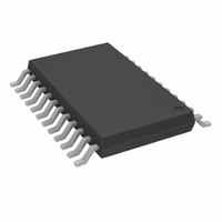
AD8185ARU-REEL7 Analog Devices Inc, AD8185ARU-REEL7 Datasheet - Page 10

AD8185ARU-REEL7
Manufacturer Part Number
AD8185ARU-REEL7
Description
IC MULTIPLEXER TRPL 2X1 24TSSOP
Manufacturer
Analog Devices Inc
Datasheet
1.AD8183ARUZ-REEL.pdf
(16 pages)
Specifications of AD8185ARU-REEL7
Rohs Status
RoHS non-compliant
Function
Multiplexer
Circuit
3 x 2:1
Voltage Supply Source
Dual Supply
Voltage - Supply, Single/dual (±)
±4.5 V ~ 5.5 V
Current - Supply
25mA
Operating Temperature
-40°C ~ 85°C
Mounting Type
Surface Mount
Package / Case
24-TSSOP (0.173", 4.40mm Width)
AD8183/AD8185
THEORY OF OPERATION
The AD8183 (G = +1) and AD8185 (G = +2) are triple-output,
2:1 multiplexers with TTL-compatible global input switching
and output enable control. Optimized for selecting between two
RGB (red, green, blue) video sources, the devices have high
peak slew rates, maintaining their bandwidth for large signals.
Additionally, the multiplexers are compensated for high phase
margin, minimizing overshoot for good pixel resolution. The
multiplexers also have video specifications that are suitable for
switching NTSC or PAL composite signals.
The multiplexers are organized as three independent channels,
each with two input transconductance stages and one output
transimpedance stage. The appropriate input transconductance
stages are selected via one logic pin (SELECT A/B), such that
all three outputs switch input connections simultaneously. The
unused input stages are disabled with a “t-switch” scheme to
provide excellent crosstalk isolation between “on” and “off”
inputs. No additional input buffering is necessary, resulting in
low input capacitance and high input impedance without addi-
tional signal degradation.
The transconductance stages, NPN differential pairs, source
signal current into the folded cascode output stages. Each out-
put stage contains a compensating network and emitter follower
output buffer. Internal voltage feedback sets the gain with the
AD8183 being configured as a unity gain follower, and the
AD8185 as a gain-of-two amplifier with a feedback network.
This architecture provides drive for a reverse-terminated video
load (150
relatively low power consumption. Careful chip design and
layout allow excellent crosstalk isolation between channels.
One logic pin OE controls whether the three outputs are
enabled, or disabled to a high-impedance state. The high
impedance disable allows larger matrices to be built when
busing the outputs together. Also, when not in use the outputs
can be disabled to reduce power consumption. In the case of
the AD8185 (G = +2), a feedback isolation scheme is used so
that the impedance of the gain-of-two feedback network does
not load the output.
Note that full power bandwidth for an undistorted sinusoidal
signal is often calculated using peak slew rate from the equation:
Peak slew rate is not the same as average slew rate (25% to 75%)
as typically specified. For a natural response, peak slew rate
may be 2.7 times larger than average slew rate. Therefore, calcu-
lating a full power bandwidth with a specified average slew rate
will give a pessimistic result.
APPLICATIONS
Driving Capacitive Loads
When driving a large capacitive load, most amplifiers will exhibit
peaking/ringing in pulse response. To minimize peaking, and to
ensure stability for larger values of capacitive loads, a small
resistor, R
capacitor, C
Full Power Bandwidth
S
, can be added between the output and the load
L
) with low differential gain and phase error for
. This is shown in Figure 39.
(
2
Peak Slew Rate
Sinusoid Amplitude
)
–10–
Power Supply and Layout Considerations
The AD8183 and AD8185 are very high performance muxes
that require attention to several important design details to real-
ize their specified performance. Good high-frequency layout
rules must be carefully observed.
A good design will start with a solid ground plane. All the GND
pins of the part(s) should be directly connected to it. In addi-
tion, bypass capacitors should be connected from each supply
pin (V
0.01 F surface-mount chip capacitors as close to the IC as
possible to provide high-frequency bypassing.
For lower frequency bypassing, higher value tantalum capacitors—
at least 10 F—should be provided from both V
ground. These do not have to be as close to the IC pins, because
parasitic inductance is not as big a factor at low frequencies.
Please refer to AD8183/AD8185 Evaluation Board Operation
Guide for further information.
Crosstalk
In normal operation the AD8183 and AD8185 will have signals
at some of the input pins that are not switched to appear at the
output. In addition, several signal paths will in general be active
at one time. In any system that has high-frequency signals that
are brought together in close proximity, there will be inevitable
crosstalk, whereby some fraction of the undesired signals will
appear at the outputs. This can result, for example, in ghost images
in an RGB monitor muxing application.
The AD8183 and AD8185 are capable of excellent low-
crosstalk performance. However, in order to realize the best
possible crosstalk performance, certain design details should be
followed. Most of the low-crosstalk specification is inherent in
the part and will result from observing the power supply and
layout consideration discussed above. This is because each of
the input and output pins are separated by at least either a
supply pin or a ground pin.
This package architecture helps the crosstalk performance in at
least three ways. First, the supply and ground pins provide extra
physical separation between the input- and output-signal pins.
Physical separation is a very effective technique for reducing
crosstalk.
Second, the supply and ground pins are at ac ground, and there-
fore provide a degree of shielding between the signals. This
works for both capacitive crosstalk, which is due to voltages on
the signals, and inductive crosstalk, which is due to currents that
flow through the signal paths.
Figure 39. Pulse Responses Driving Capacitive Loads
CC
and V
–0.5V
0.5V
0.0V
EE
) to the ground plane. It is suggested to use
R
S
= 0 , C
250mV
R
R
L
S
S
= 5pF
= 15 , C
= 20 , C
75
V
IN
L
L
= 20pF
= 20pF
R
C
S
L
5ns
1k
V
OUT
CC
and V
REV. 0
EE
to


