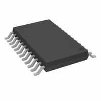
AD8185ARU-REEL7 Analog Devices Inc, AD8185ARU-REEL7 Datasheet - Page 12

AD8185ARU-REEL7
Manufacturer Part Number
AD8185ARU-REEL7
Description
IC MULTIPLEXER TRPL 2X1 24TSSOP
Manufacturer
Analog Devices Inc
Datasheet
1.AD8183ARUZ-REEL.pdf
(16 pages)
Specifications of AD8185ARU-REEL7
Rohs Status
RoHS non-compliant
Function
Multiplexer
Circuit
3 x 2:1
Voltage Supply Source
Dual Supply
Voltage - Supply, Single/dual (±)
±4.5 V ~ 5.5 V
Current - Supply
25mA
Operating Temperature
-40°C ~ 85°C
Mounting Type
Surface Mount
Package / Case
24-TSSOP (0.173", 4.40mm Width)
AD8183/AD8185
result, the input and output traces, in addition to having a con-
trolled impedance, are well shielded.
SEL A/B AND OE
SEL A/B (Pin 22 of the device) allows the A or B inputs to be
selected.
When SEL A/B is at logic low, (equal to or less than 0.8 V),
inputs 0A, 1A and 2A are directed to OUTPUTs 0, 1, and 2,
respectively. When SEL A/B is at logic high, (equal to or greater
than 2.0 V), inputs 0B, 1B, and 2B are directed to OUTPUTs
0, 1, and 2, respectively.
There are two ways to provide SEL A/B to the device: using a
jumper or a BNC connection. With the jumper in the W4 posi-
tion, SEL A/B is tied to ground. This selects the A inputs.
With the jumper in the W3 position, SEL A/B is tied to 5 V,
through pull up resistor R15. This selects the B inputs.
If faster use of SEL A/B is desired, the 50
J10 can be used. If J10 is used, there must NOT be a jumper on
W3 and W4. Microstrip line techniques provide a 50
teristic impedance from J10 to the device. Please refer to Figure
IN0A
IN1A
IN2A
IN2B
IN1B
IN0B
J1
J2
J3
J4
J5
J6
AGND
AGND
AGND
AGND
AGND
AGND
75
75
75
75
75
75
R1
R2
R3
R4
R5
R6
75
75
75
75
75
75
V
STRIPLINE
STRIPLINE
STRIPLINE
V
STRIPLINE
STRIPLINE
STRIPLINE
CC
EE
OE
AGND
J11
C7
0.01 F
OE
AGND
C8
0.01 F
W2
W1
BNC connector at
Figure 42. Evaluation Board Schematic
V
CC
DGND
AGND
AGND
AGND
DGND
R16
20k
10
11
12
1
2
3
4
5
6
7
8
9
50
charac-
AGND
IN0A
DGND
IN1A
AGND
IN2A
V
V
IN2B
AGND
IN1B
AGND
IN0B
V
CC
EE
CC
DGND
AGND
MICROSTRIP LINE
DVCC
V
V
CC
AD8183/
EE
AD8185
DUT
W5
P1
P1
P1
P1
P1
SEL A/B
–12–
DGND
1
2
4
5
6
AGND
DVCC
R11
50
OPTIONAL
C15
0.01 F
OUT0
OUT1
OUT2
DGND
V
V
V
V
V
V
OE
CC
CC
EE
CC
EE
CC
DGND
AGND
41 for the arrangement of the PCB layers. If J10 is used, the
user may wish to install a 50
OE (Pin 23 of the device) allows the three outputs to be enabled
or disabled. When OE is at logic low, (equal to or less than
0.8 V), Outputs 0, 1, and 2 are enabled. When OE is at logic
high, (equal to or greater than 2.0 V), Outputs 0, 1, and 2 are
disabled (placed into a high impedance state).
Once again, there are two different ways to provide OE to the
device: using a jumper or a BNC connection. With the jumper
in the W2 position, OE is tied to ground. This enables the outputs.
With the jumper in the W1 position, OE is tied to 5 V, through
pull-up resistor R16. This selects “Hi Z,” or high impedance,
and the outputs are disabled.
If faster use of OE is desired, the 50
can be used. If J11 is used, there must NOT be a jumper on W1
and W2. Microstrip line techniques provide a 50
tic impedance from J11 to the device. Please refer to Figure 41
for the arrangement of the PCB layers. If J11 is used, the user
may wish to install a 50
DVCC
V
V
24
23
22
21
20
19
18
17
16
15
14
13
CC
EE
+
+
+
DGND
AGND
AGND
C2
10 F
C3
10 F
C1
10 F
AGND
C9
0.01 F
DGND
AGND
AGND
C6
0.1 F
C5
0.1 F
C4
0.1 F
DGND
C10
0.01 F
DGND
V
AGND
V
DVCC
EE
CC
50
MICROSTRIP LINE
AGND
AGND
AGND
AGND
DGND
R10
50
OPTIONAL
C14
0.01 F
C13
0.01 F
C12
0.01 F
C11
0.01 F
V
V
V
V
DVCC
V
termination resistor at R11.
CC
EE
CC
EE
CC
R14
75
R13
75
R12
75
termination resistor at R10.
V
75
75
75
CC
DGND
R15
20k
STRIPLINE
STRIPLINE
STRIPLINE
W3
W4
BNC connector at J11
SEL A/B
J10
J9
J8
J7
characteris-
OUT0
OUT1
OUT2
SEL A/B
REV. 0


