ADG333ABNZ Analog Devices Inc, ADG333ABNZ Datasheet
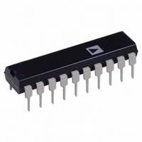
IC SWITCH QUAD SPDT 20DIP

ADG333ABNZ

Manufacturer Part Number
ADG333ABNZ
Description
IC SWITCH QUAD SPDT 20DIP
Manufacturer
Analog Devices Inc
Type
Analog Switchr
Datasheet

Specifications of ADG333ABNZ

Function
Switch
Circuit
4 x SPDT
On-state Resistance
45 Ohm
Voltage Supply Source
Single Supply
Voltage - Supply, Single/dual (±)
12V
Current - Supply
0.01µA
Operating Temperature
-40°C ~ 85°C
Mounting Type
Through Hole
Package / Case
20-DIP (0.300", 7.62mm)
Analog Switch Type
SPDT
No. Of Channels
4
On State Resistance Max
45ohm
Turn Off Time
80ns
Turn On Time
90ns
Supply Voltage Range
3V To 30V
Operating Temperature Range
-40°C To +85°C
Multiplexer Configuration
Quad SPDT
Number Of Inputs
4
Number Of Outputs
8
Number Of Channels
4
Analog Switch On Resistance
45@±15VOhm
Analog Switch Turn On Time
110ns
Analog Switch Turn Off Time
100ns
Package Type
PDIP N
Power Supply Requirement
Single/Dual
Single Supply Voltage (min)
3V
Single Supply Voltage (typ)
12V
Single Supply Voltage (max)
30V
Dual Supply Voltage (min)
±3V
Dual Supply Voltage (typ)
±5/±9/±12/±15V
Dual Supply Voltage (max)
±20V
Power Dissipation
3.77mW
Supply Current
0.25@±15VmA
Mounting
Through Hole
Pin Count
20
Operating Temp Range
-40C to 85C
Operating Temperature Classification
Industrial
Package
20PDIP N
Maximum On Resistance
45@±15V Ohm
Maximum High Level Output Current
20 mA
Maximum Turn-off Time
100(Typ)@12V ns
Maximum Turn-on Time
110(Typ)@12V ns
Switch Architecture
SPDT
Power Supply Type
Single|Dual
Lead Free Status / RoHS Status
Lead free / RoHS Compliant
Lead Free Status / RoHS Status
Lead free / RoHS Compliant, Lead free / RoHS Compliant

Available stocks

Company
Part Number
Manufacturer
Quantity
Price
Part Number:
ADG333ABNZ
Manufacturer:
ADI/亚德诺
Quantity:
20 000
FEATURES
44 V supply maximum ratings
V
Low on resistance (45 Ω max)
Low ∆R
Low R
Low power dissipation
Fast switching times
Low leakage currents (5 nA max)
Low charge injection (10 pC max)
Break-before-make switching action
APPLICATIONS
Audio and video switching
Battery-powered systems
Test equipment
Communication systems
GENERAL DESCRIPTION
The ADG333A is a monolithic CMOS device comprising four
independently selectable SPDT switches. It is designed on an
LC
achieves a high switching speed and a low on resistance.
The on resistance profile is very flat over the full analog input
range, ensuring good linearity and low distortion when
switching audio signals. High switching speed also makes the
part suitable for video signal switching. CMOS construction
ensures ultralow power dissipation, making the part ideally
suited for portable, battery-powered instruments.
When they are on, each switch conducts equally well in both
directions and has an input signal range that extends to the
power supplies. In the off condition, signal levels up to the
supplies are blocked. All switches exhibit break-before-make
switching action for use in multiplexer applications. Inherent
in the design is low charge inject
Rev. A
Information furnished by Analog Devices is believed to be accurate and reliable.
However, no responsibility is assumed by Analog Devices for its use, nor for any
infringements of patents or other rights of third parties that may result from its use.
Specifications subject to change without notice. No license is granted by implication
or otherwise under any patent or patent rights of Analog Devices. Trademarks and
registered trademarks are the property of their respective owners.
SS
t
t
2
ON
OFF
to V
MOS process, which provides low power dissipation yet
< 175 ns
ON
< 145 ns
DD
ON
match (4 Ω max)
analog signal range
(5 Ω max)
PRODUCT HIGHLIGHTS
1.
2.
3.
4.
One Technology Way, P.O. Box 9106, Norwood, MA 02062-9106, U.S.A.
Tel: 781.329.4700
Fax: 781.461.3113
Extended signal range.
The ADG333A is fabricated on an enhanced LC
process, giving an increased signal range which extends to
the supply rails.
Low power dissipation.
Low R
Single-supply operation.
For applications where the analog signal is unipolar, the
ADG333A can be operated from a single rail power supply.
The part is fully specified with a single 12 V supply.
ON
FUNCTIONAL BLOCK DIAGRAM
.
SWITCHES SHOWN FOR A LOGIC 1 INPUT
S1A
S1B
S2B
S2A
IN1
IN2
D1
D2
© 2005 Analog Devices, Inc. All rights reserved.
ADG333A
Quad SPDT Switch
Figure 1.
S4A
D2
S4B
IN4
IN3
S3B
D3
S3A
ADG333A
www.analog.com
2
MOS

Related parts for ADG333ABNZ

ADG333ABNZ Summary of contents

Page 1

FEATURES 44 V supply maximum ratings analog signal range SS DD Low on resistance (45 Ω max) Low ∆R (5 Ω max) ON Low R match (4 Ω max) ON Low power dissipation Fast switching times t ...

Page 2

ADG333A TABLE OF CONTENTS Specifications..................................................................................... 3 Dual Supply ................................................................................... 3 Single Supply ................................................................................. 4 Absolute Maximum Ratings............................................................ 5 ESD Caution.................................................................................. 5 Terminology ...................................................................................... 6 Pin Configurations and Function Descriptions ........................... 7 REVISION HISTORY 3/05—Rev Rev. A Updated Format..................................................................Universal ...

Page 3

SPECIFICATIONS DUAL SUPPLY −15 V, GND = 0 V, unless otherwise noted Table 1. Parameter ANALOG SWITCH Analog Signal Range R ON ∆ Match ON LEAKAGE CURRENTS Source OFF Leakage ...

Page 4

ADG333A SINGLE SUPPLY ± 10%, GND = 0 V, unless otherwise noted Table 2. Parameter ANALOG SWITCH Analog Signal Range RON LEAKAGE CURRENTS Source OFF Leakage I (OFF) S Channel ...

Page 5

ABSOLUTE MAXIMUM RATINGS T = 25°C unless otherwise noted. A Table 3. Parameter Min + GND –0 + GND +0 – ...

Page 6

ADG333A TERMINOLOGY R ON Ohmic resistance between D and S. ∆ variation due to a change in the analog input voltage with a ON constant load current. R Match ON Difference between the R of any two channels. ...

Page 7

PIN CONFIGURATIONS AND FUNCTION DESCRIPTIONS IN1 IN4 1 20 S1A S4A ADG333A S1B S4B 4 17 TOP VIEW (Not to Scale GND S2B S3B 7 ...

Page 8

ADG333A TYPICAL PERFORMANCE CHARACTERISTICS 25° + – +10V –10V +15V –15V SS 10 –15 –10 ...

Page 9

C = 10nF +16. –16. +12V DD – –10 –15 –20 –15 –10 – (V) S Figure 11. Charge ...

Page 10

ADG333A TEST CIRCUITS Figure 14. On Resistance V DD 0.1µ –10V +10V IN V GND SS 0.1µF V ...

Page 11

APPLICATION INFORMATION ADG333A SUPPLY VOLTAGES The ADG333A can operate from a dual or signal supply. V should be connected to GND when operating with a single supply. When using a dual supply, the ADG333A can also operate with unbalanced supplies; ...

Page 12

ADG333A OUTLINE DIMENSIONS 1.060 (26.92) 1.030 (26.16) 0.980 (24.89 0.280 (7.11) 0.250 (6.35) 1 0.240 (6.10) 10 PIN 1 0.100 (2.54) BSC 0.060 (1.52) 0.210 (5.33) MAX 0.015 0.150 (3.81) (0.38) 0.015 (0.38) MIN 0.130 (3.30) 0.115 (2.92) ...

Related keywords