ADG438FBR Analog Devices Inc, ADG438FBR Datasheet
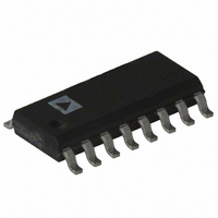
IC MULTIPLEXER 8X1 16SOIC

ADG438FBR

Manufacturer Part Number
ADG438FBR
Description
IC MULTIPLEXER 8X1 16SOIC
Manufacturer
Analog Devices Inc
Type
Analog Multiplexerr
Datasheet

Specifications of ADG438FBR

Rohs Status
RoHS non-compliant
Function
Multiplexer
Circuit
1 x 8:1
On-state Resistance
400 Ohm
Current - Supply
0.05mA
Operating Temperature
-40°C ~ 85°C
Mounting Type
Surface Mount
Package / Case
16-SOIC (0.154", 3.90mm Width)
Package
16SOIC N
Maximum On Resistance
400@±15V Ohm
Maximum Propagation Delay Bus To Bus
220@±15V ns
Maximum High Level Output Current
20 mA
Multiplexer Architecture
8:1
Maximum Turn-off Time
150@±15V ns
Maximum Turn-on Time
250@±15V ns
Power Supply Type
Single|Dual

Available stocks

Company
Part Number
Manufacturer
Quantity
Price
Part Number:
ADG438FBR
Quantity:
993
Part Number:
ADG438FBR
Manufacturer:
ADI/亚德诺
Quantity:
20 000
Part Number:
ADG438FBRN
Manufacturer:
ADI/亚德诺
Quantity:
20 000
Part Number:
ADG438FBRZ
Manufacturer:
ADI
Quantity:
3 491
Part Number:
ADG438FBRZ
Manufacturer:
ADI/亚德诺
Quantity:
20 000
a
GENERAL DESCRIPTION
The ADG438F/ADG439F are CMOS analog multiplexers, the
ADG438F comprising 8 single channels and the ADG439F
comprising four differential channels. These multiplexers pro-
vide fault protection. Using a series n-channel, p-channel, n-
channel MOSFET structure, both device and signal source
protection is provided in the event of an overvoltage or power
loss. The multiplexer can withstand continuous overvoltage
inputs from –40 V to +55 V. During fault conditions, the multi-
plexer input (or output) appears as an open circuit and only a
few nanoamperes of leakage current will flow. This protects not
only the multiplexer and the circuitry driven by the multiplexer,
but also protects the sensors or signal sources which drive the
multiplexer.
The ADG438F switches one of eight inputs to a common out-
put as determined by the 3-bit binary address lines A0, A1 and
A2. The ADG439F switches one of four differential inputs to a
common differential output as determined by the 2-bit binary
address lines A0 and A1. An EN input on each device is used to
enable or disable the device. When disabled, all channels are
switched OFF.
REV. D
Information furnished by Analog Devices is believed to be accurate and
reliable. However, no responsibility is assumed by Analog Devices for its
use, nor for any infringements of patents or other rights of third parties
which may result from its use. No license is granted by implication or
otherwise under any patent or patent rights of Analog Devices.
FEATURES
Fast Switching Times
Fault and Overvoltage Protection (–40 V, +55 V)
All Switches OFF with Power Supply OFF
Analog Output of ON Channel Clamped Within Power
Latch-Up Proof Construction
Break Before Make Construction
TTL and CMOS Compatible Inputs
APPLICATIONS
Data Acquisition Systems
Industrial and Process Control Systems
Avionics Test Equipment
Signal Routing Between Systems
High Reliability Control Systems
t
t
Supplies If an Overvoltage Occurs
ON
OFF
250 ns max
150 ns max
Fault-Protected Analog Multiplexers
PRODUCT HIGHLIGHTS
1. Fault Protection.
2. ON channel turns OFF while fault exists.
3. Low R
4. Fast Switching Times.
5. Break-Before-Make Switching.
6. Trench Isolation Eliminates Latch-up.
7. Improved OFF Isolation.
One Technology Way, P.O. Box 9106, Norwood, MA 02062-9106, U.S.A.
Tel: 781/329-4700
Fax: 781/326-8703
High Performance 4/8 Channel
S8
S1
The ADG438F/ADG439F can withstand continuous volt-
age inputs up to –40 V or +55 V. When a fault occurs due
to the power supplies being turned off, all the channels
are turned off and only a leakage current of a few nano-
amperes flows.
Switches are guaranteed break-before-make so that input
signals are protected against momentary shorting.
A dielectric trench separates the p- and n-channel MOSFETs
thereby preventing latch-up.
Trench isolation enhances the channel-to-channel isolation
of the ADG438F/ADG439F.
A0
DECODER
ADG438F
ON.
A1 A2 EN
1 OF 8
FUNCTIONAL BLOCK DIAGRAMS
ADG438F/ADG439F
World Wide Web Site: http://www.analog.com
D
S1A
S4A
S1B
S4B
© Analog Devices, Inc., 2000
DECODER
A0
ADG439F
1 OF 4
A1 EN
DA
DB

Related parts for ADG438FBR

ADG438FBR Summary of contents

Page 1

FEATURES Fast Switching Times t 250 ns max ON t 150 ns max OFF Fault and Overvoltage Protection (–40 V, +55 V) All Switches OFF with Power Supply OFF Analog Output of ON Channel Clamped Within Power Supplies If ...

Page 2

ADG438F/ADG439F–SPECIFICATIONS Dual Supply ( –15 V, GND = 0 V, unless otherwise noted Parameter +25 C ANALOG SWITCH Analog Signal Range Drift 0 Match 3 ON ...

Page 3

... Exposure to absolute maximum rating conditions for extended periods may affect device reliability. Only one absolute maximum rating may be applied at any one time. ORDERING GUIDE Model Temperature Range ADG438FBN – +105 C ADG438FBR – +105 C ADG439FBN – +105 C ADG439FBR – +105 C ADG439FBRW – +105 Plastic DIP ...

Page 4

ADG438F/ADG439F TERMINOLOGY V Most positive power supply potential Most negative power supply potential. SS GND Ground (0 V) reference. R Ohmic resistance between D and variation due to a change in the analog ON ...

Page 5

C 500 +85 C 250 0 –15 –10 – – Volts D S Figure 4. On Resistance as a Function of V Different Temperatures 1m 100 10 1 100n ...

Page 6

ADG438F/ADG439F THEORY OF OPERATION The ADG438F/ADG439F multiplexers are capable of with- standing overvoltages from – +55 V, irrespective of whether the power supplies are present or not. Each channel of the multiplexer consists of an n-channel MOSFET, a ...

Page 7

(ON +2. Test Circuit 4. I (ON THRU S7 A0 ADG438F ...

Page 8

ADG438F/ADG439F ADG438F GND * SIMILAR CONNECTION FOR ADG439F ADG438F GND ...

Related keywords