HCF4051M013TR STMicroelectronics, HCF4051M013TR Datasheet
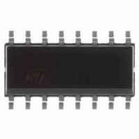
IC MUX/DEMUX 8X1 16SOIC

HCF4051M013TR

Manufacturer Part Number
HCF4051M013TR
Description
IC MUX/DEMUX 8X1 16SOIC
Manufacturer
STMicroelectronics
Series
4000r
Type
Analog Multiplexerr
Datasheet

Specifications of HCF4051M013TR

Function
Multiplexer/Demultiplexer
Circuit
1 x 8:1
On-state Resistance
280 Ohm
Voltage Supply Source
Dual Supply
Voltage - Supply, Single/dual (±)
±3 V ~ 20 V
Current - Supply
.08µA
Operating Temperature
-55°C ~ 125°C
Mounting Type
Surface Mount
Package / Case
16-SOIC (0.154", 3.90mm Width)
Number Of Channels
1 Channel
On Resistance (max)
1050 Ohms
Propagation Delay Time
60 ns
On Time (max)
720 ns
Off Time (max)
450 ns
Supply Voltage (max)
20 V
Supply Voltage (min)
3 V
Maximum Power Dissipation
200 mW
Maximum Operating Temperature
+ 125 C
Minimum Operating Temperature
- 55 C
Mounting Style
SMD/SMT
Number Of Switches
1
Package
16SOP
Maximum On Resistance
1050@5V Ohm
Maximum Propagation Delay Bus To Bus
20@15V|30@10V|60@5V ns
Multiplexer Architecture
8:1
Maximum Turn-off Time
450@5V ns
Maximum Turn-on Time
720@5V ns
Power Supply Type
Single
Lead Free Status / RoHS Status
Lead free / RoHS Compliant
Other names
497-1129-2

Available stocks

Company
Part Number
Manufacturer
Quantity
Price
Part Number:
HCF4051M013TR
Manufacturer:
ST
0
Company:
Part Number:
HCF4051M013TR
Quantity:
82
Part Number:
HCF4051M013TR/HCF4052M013TR
Manufacturer:
ST
Quantity:
20 000
PIN CONNECTION
October 2002
LOW "ON" RESISTANCE : 125
OVER 15V p.p SIGNAL-INPUT RANGE FOR
V
HIGH "OFF" RESISTANCE : CHANNEL
LEAKAGE
BINARY ADDRESS DECODING ON CHIP
HIGH DEGREE OF LINEARITY : < 0.5%
DISTORTION TYP. at f
V
VERY LOW QUIESCENT POWER
DISSIPATION UNDER ALL DIGITAL
CONTROL INPUT AND SUPPLY
CONDITIONS : 0.2 W (Typ.)
at V
MATCHED SWITCH CHARACTERISTICS :
R
WIDE RANGE OF DIGITAL AND ANALOG
SIGNAL LEVELS : DIGITAL 3 to 20,
ANALOG TO 20V p.p.
QUIESCENT CURRENT SPECIFIED UP TO
20V
5V, 10V AND 15V PARAMETRIC RATINGS
INPUT LEAKAGE CURRENT
I
100% TESTED FOR QUIESCENT CURRENT
MEETS ALL REQUIREMENTS OF JEDEC
JESD13B " STANDARD SPECIFICATIONS
FOR DESCRIPTION OF B SERIES CMOS
DEVICES"
I
DD
DD
ON
= 100nA (MAX) AT V
DD
- V
- V
= 5 (Typ.) FOR V
- V
EE
SS
SS
= 15V
> 10V, RL = 10K
= V
100pA (Typ.) at V
DD
- V
EE
DD
IS
DD
= 1KHz, V
=10V
= 18V T
- V
ANALOG MULTIPLEXER/DEMULTIPLEXER
EE
DD
= 15V
A
(Typ.)
- V
= 25°C
IS
EE
= 5 V
= 18V
pp
,
ORDER CODES
DESCRIPTION
The HCF4051B is a monolithic integrated circuit
fabricated
technology available in DIP and SOP packages.
The HCF4051B analog multiplexer/demultiplexer
is a digitally controlled analog switch having low
ON impedance and very low OFF leakage current.
This multiplexer circuit dissipate extremely low
quiescent power over the full V
V
logic state of the control signals.
When a logic "1" is present at the inhibit input
terminal all channel are off. This device is a single
8-channel multiplexer having three binary control
inputs, A, B, and C, and an inhibit input. The three
binary signals select 1 of 8 channels to be turned
on, and connect one of the 8 inputs to the output.
PACKAGE
EE
SOP
DIP
supply voltage range, independent of the
in
DIP
HCF4051BM1
HCF4051BEY
SINGLE 8-CHANNEL
Metal
TUBE
Oxide
HCF4051B
DD
HCF4051M013TR
SOP
- V
Semiconductor
SS
T & R
and V
DD
1/10
-

Related parts for HCF4051M013TR

HCF4051M013TR Summary of contents

Page 1

... A, B, and C, and an inhibit input. The three binary signals select channels to be turned on, and connect one of the 8 inputs to the output. HCF4051B SINGLE 8-CHANNEL DIP SOP TUBE HCF4051BEY HCF4051BM1 HCF4051M013TR in Metal Oxide Semiconductor - V DD supply voltage range, independent of the T & R and V - ...

Page 2

HCF4051B INPUT EQUIVALENT CIRCUIT TRUTH TABLE INPUT STATES INHIBIT FUNCTIONAL DIAGRAM 2/10 PIN DESCRIPTION PIN No 11, 10 13, 14, 15, 12 ...

Page 3

ABSOLUTE MAXIMUM RATINGS Symbol V Supply Voltage Input Voltage Input Current I P Power Dissipation per Package D Power Dissipation per Output Transistor T Operating Temperature op T Storage Temperature stg Absolute Maximum Ratings ...

Page 4

HCF4051B DC SPECIFICATIONS Symbol Parameter V (V) I Quiescent Device L Current (all switches ON or all switches OFF) SWITCH R Resistance ON 0 < Resistance ON RON 0 < V (between any switches) ...

Page 5

DYNAMIC ELECTRICAL CHARACTERISTICS (T fall time = Parameter Propagation Delay Time (signal input to output) Frequency Response Channel "ON" (sine = V wave input log ...

Page 6

HCF4051B TYPICAL BIAS VOLTAGES The ADDRESS (digtal-control inputs) and INHIBIT logic levels are : "0"=V from SPECIAL CONSIDERATIONS Control of analog signals up to 20V peak to peak can be achieved by digital signal amplitudes ...

Page 7

WAVEFORM 1 : CHANNEL BEING TURNED ON (R WAVEFORM 2 : CHANNEL BEING TURNED OFF ( f=1MHz; 50% duty cycle f=1MHz; 50% duty cycle) L HCF4051B 7/10 ...

Page 8

HCF4051B DIM. MIN. a1 0. 8/10 Plastic DIP-16 (0.25) MECHANICAL DATA mm. TYP MAX. 1.65 0.5 0.25 20 8.5 2.54 17.78 7.1 5.1 3.3 1.27 inch MIN. TYP. ...

Page 9

SO-16 MECHANICAL DATA mm. DIM. MIN 0 0. 9 3.8 G 4 TYP MAX. MIN. 1.75 0.2 0.003 1.65 0.46 0.013 0.25 ...

Page 10

... No license is granted by implication or otherwise under any patent or patent rights of STMicroelectronics. Specifications mentioned in this publication are subject to change without notice. This publication supersedes and replaces all information previously supplied ...

Related keywords