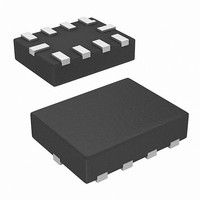
ISL54222AIRUZ-T Intersil, ISL54222AIRUZ-T Datasheet

ISL54222AIRUZ-T
Specifications of ISL54222AIRUZ-T
Related parts for ISL54222AIRUZ-T
ISL54222AIRUZ-T Summary of contents
Page 1
... CAUTION: These devices are sensitive to electrostatic discharge; follow proper IC Handling Procedures. | 1-888-INTERSIL or 1-888-468-3774 Intersil (and design registered trademark of Intersil Americas Inc. Copyright Intersil Americas Inc. 2009, 2010. All Rights Reserved All other trademarks mentioned are the property of their respective owners 4.4Ω ...
Page 2
Pin Configurations ISL54222A (10 LD 1.8X1.4 µTQFN) TOP VIEW HSD1- HSD2 VDD 9 SEL HSD1+ HSD2+ ISL54222A (10 LD 3X3 TDFN) TOP VIEW PD LOGIC SEL 1 CONTROL HSD1+ 2 HSD2 ...
Page 3
... Ordering Information PART NUMBER (Note 5) MARKING ISL54222AIRUZ-T (Notes ISL54222AIRU1Z-T (Notes ISL54222AIRTZ (Note 3) 222A ISL54222AIRTZ-T (Notes 2, 3) 222A ISL54222AIUZ (Note 3) 4222A ISL54222AIUZ-T (Notes 2, 3) 4222A ISL54222AIRUEVAL1Z Evaluation Board NOTES: 2. Please refer to TB347 for details on reel specifications. 3. These Intersil Pb-free plastic packaged products employ special Pb-free material sets, molding compounds/die attach materials, and 100% matte tin plate plus anneal (e3 termination finish, which is RoHS compliant and compatible with both SnPb and Pb-free soldering operations) ...
Page 4
... Ld 2.1x1.6 µTQFN (Notes 7, 10 1.8x1.4 µTQFN (Notes 7, 10) Maximum Junction Temperature (Plastic Package). . Maximum Storage Temperature Range -65°C to +150°C Pb-Free Reflow Profile . . . . . . . . . . . . . . . . . .see link below http://www.intersil.com/pbfree/Pb-FreeReflow.asp Operating Conditions Temperature Range . . . . . . . . . . . . . . . . . . -40°C to +85°C V Supply Voltage Range . . . . . . . . . . . . . . . 1.8V to 3.3V DD Logic Control Input Voltage ...
Page 5
Electrical Specifications - 1.8V to 3.3V Supply PARAMETER ON Leakage Current 3.3V, SEL = 0.3V, 3V, V HSD2x(ON HSD1X Power OFF Leakage Current 0V 5.25V ...
Page 6
Electrical Specifications - 1.8V to 3.3V Supply PARAMETER Positive Supply Current 1.8V, SEL = 0V Positive Supply Current 1.8V, SEL = 0V (Low Power ...
Page 7
Test Circuits and Waveforms V DD LOGIC INPUT 0V SWITCH OUTPUT V OUT 0V FIGURE 2A. MEASUREMENT POINTS V Repeat test for all switches. 7 ISL54222A (Continued) V INPUT 10 Repeat test for all switches. C capacitance. FIGURE ...
Page 8
Test Circuits and Waveforms HSDxx IMPEDANCE ANALYZER Dx GND Repeat test for all switches. FIGURE 4. CAPACITANCE TEST CIRCUIT t ri 90% 50% 10% DIN+ t skew_i DIN- 90% 50% 10 90% 10% 50% OUT+ t ...
Page 9
Application Block Diagram V BUS D- D+ GND Detailed Description The ISL54222A device is a dual single pole/double throw (SPDT) analog switch configured as a DPDT that operates from a single DC power supply in the range of 1.8V to ...
Page 10
During the fault condition normal operation is not guaranteed until the fault is removed. See the following “USB 2.0 ...
Page 11
Typical Performance Curves 6 40mA COM 5.5 1.8V 5.0 2.7V 4.5 3.3V 4.0 3.5 3.0 0 0.1 0.2 V (V) COM FIGURE 7. ON-RESISTANCE vs SUPPLY VOLTAGE vs SWITCH VOLTAGE 1. 40mA COM ...
Page 12
Typical Performance Curves V = 1.8V DD FIGURE 13. EYE PATTERN: 480Mbps WITH USB SWITCHES IN THE SIGNAL PATH 12 ISL54222A T = +25°C, Unless Otherwise Specified (Continued) A TIME SCALE (0.2ns/DIV) FN6902.1 February 4, 2010 ...
Page 13
Typical Performance Curves V = 1.8V DD FIGURE 14. EYE PATTERN: 12Mbps WITH USB SWITCHES IN THE SIGNAL PATH V = 3.3V DD FIGURE 15. EYE PATTERN: 12Mbps WITH USB SWITCHES IN THE SIGNAL PATH 13 ISL54222A T = +25°C, ...
Page 14
Typical Performance Curves 50Ω 0dBm, 0.2VDC BIAS IN 1M 10M FREQUENCY (Hz) FIGURE 16. FREQUENCY RESPONSE -20 -30 -40 -50 -60 -70 -80 -90 -100 -110 0.001M 0.01M 0.1M ...
Page 15
... Initial Release. Products Intersil Corporation is a leader in the design and manufacture of high-performance analog semiconductors. The Company's products address some of the industry's fastest growing markets, such as, flat panel displays, cell phones, handheld products, and notebooks. Intersil's product families address power management and analog signal processing functions ...
Page 16
... Dimensions D2 and E2 are for the exposed pads which provide M 0. improved electrical and thermal performance. 8. Nominal dimensions are provided to assist with PCB Land Pattern Design efforts, see Intersil Technical Brief TB389. 9. Compliant to JEDEC MO-229-WEED-3 except for D2 dimensions TERMINAL TIP ( 2.90 ) MILLIMETERS ...
Page 17
... The pin #1 identifier may be either a mold or mark feature. Maximum package warpage is 0.05mm. 7. Maximum allowable burrs is 0.076mm in all directions. 8. JEDEC Reference MO-255. 9. For additional information, to assist with the PCB Land Pattern 10. Design effort, see Intersil Technical Brief TB389 10X 0. 0. ...
Page 18
... Maximum allowable burrs is 0.076mm in all directions. 9. Same as JEDEC MO-255UABD except: No lead-pull-back, "A" MIN dimension = 0.45 not 0.50mm "L" MAX dimension = 0.45 not 0.42mm. 10. For additional information, to assist with the PCB Land Pattern Design effort, see Intersil Technical Brief TB389. L MILLIMETERS NOMI- MIN NAL ...
Page 19
... Accordingly, the reader is cautioned to verify that data sheets are current before placing orders. Information furnished by Intersil is believed to be accurate and reliable. However, no responsibility is assumed by Intersil or its subsidiaries for its use; nor for any infringements of patents or other rights of third parties which may result from its use. No license is granted by implication or otherwise under any patent or patent rights of Intersil or its subsidiaries ...


