ISL54230IRTZ-T Intersil, ISL54230IRTZ-T Datasheet
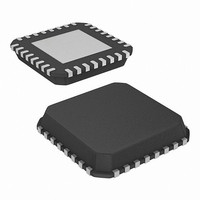
IC SWITCH QUAD DPDT 32TQFN

ISL54230IRTZ-T

Manufacturer Part Number
ISL54230IRTZ-T
Description
IC SWITCH QUAD DPDT 32TQFN
Manufacturer
Intersil
Datasheet

Specifications of ISL54230IRTZ-T

Function
Switch
Circuit
4 x DPDT
On-state Resistance
1.5 Ohm
Voltage Supply Source
Single Supply
Voltage - Supply, Single/dual (±)
2 V ~ 5.5 V
Current - Supply
1µA
Operating Temperature
-40°C ~ 85°C
Mounting Type
Surface Mount
Package / Case
32-WFQFN Exposed Pad
Lead Free Status / RoHS Status
Lead free / RoHS Compliant
Octal Multiprotocol Switch
The Intersil ISL54230 is a multiprotocol Quad Double-Pole
Double-Throw (DPDT) analog switch that can operate from a
single +2.0V to +5.5V supply. It contains eight SPDT (Single
Pole/Double Throw) switches configured into four DPDT
blocks. Each DPDT block is independently controlled by a
logic input for Normally Open (NO) or Normally Closed (NC)
switch configuration.The part is designed for switching or
routing a combination of USB High-Speed, USB Full-Speed,
digital, and analog signals in portable battery powered
products.
The digital inputs are 1.8V logic compatible when operated
with a 2.7V to 3.6V supply. The ISL54230 has two switch
enable pins to disable certain blocks of the switch. The
ISL54230 is available in a 36 ball 2.5mmx2.5mm WLCSP or a
32 Ld TQFN 5mmx5mm package. It operates over a
temperature range of -40 to +85°C.
Applications
• Cellular/Mobile Phones
• PDAs
• Digital Cameras and Camcorders
• USB/UART/Audio Switching
Block Diagram
COM1A
COM1B
COM2A
COM2B
COM3A
COM3B
COM4A
COM4B
OE1
OE2
V
IN1
IN2
IN3
IN4
DD
HS_USB
HS_USB
HS_USB
HS_USB
®
1
Data Sheet
NO1A
NC1A
NO1B
NC1B
NO2A
NC2A
NO2B
NC2B
NO3A
NC3A
NO3B
NC3B
NO4A
NC4A
NO4B
NC4B
GND
1-888-INTERSIL or 1-888-468-3774
CAUTION: These devices are sensitive to electrostatic discharge; follow proper IC Handling Procedures.
Ordering Information
ISL54230IRTZ
(Note 1)
ISL54230IRTZ-T*
(Note 1)
ISL54230IIZ-T*
(Note 2)
*Please refer to TB347 for details on reel specifications.
NOTES:
PART NUMBER
1. These Intersil Pb-free plastic packaged products employ special Pb-
2. These Intersil Pb-free WLCSP and BGA packaged products
Features
• High Speed (480Mbps) and Full Speed (12Mbps)
• Compliant with USB 2.0 Short Circuit and Overvoltage
• 1.8V Logic Compatible (+2.7V to +3.6V Supply)
• Switch Terminals Overvoltage Protected Up to +5.5V
• Enable Pin to disable Switch Blocks
• Two DPDT 1Ω/6Ω Switches
• Two DPDT USB 2.0 FS/HS Capable Switches
• USB Switch Low ON Capacitance. . . . . . . . . . . . . . . 12pF
• USB Switch Low ON-Resistance. . . . . . . . . . . . . . . . . 6Ω
• Single Supply Operation (V
• Low Power Consumption (P
• Low I+ Current when V
• Available in 36 Ball WLCSP and 32 Ld 5mmx5mm TQFN
• Pb-Free (RoHS Compliant)
Signaling Capability per USB 2.0
Requirements Without Additional External Components
Package
free material sets, molding compounds/die attach materials, and
100% matte tin plate plus anneal (e3 termination finish, which is
RoHS compliant and compatible with both SnPb and Pb-free
soldering operations). Intersil Pb-free products are MSL classified
at Pb-free peak reflow temperatures that meet or exceed the Pb-
free requirements of IPC/JEDEC J STD-020.
products employ special Pb-free material sets; molding
compounds/die attach materials and SnAgCu - e1 solder ball
terminals, which are RoHS compliant and compatible with both
SnPb and Pb-free soldering operations. Intersil Pb-free WLCSP
and BGA packaged products are MSL classified at Pb-free peak
reflow temperatures that meet or exceed the Pb-free requirements
of IPC/JEDEC J STD-020.
All other trademarks mentioned are the property of their respective owners.
May 28, 2009
|
Intersil (and design) is a registered trademark of Intersil Americas Inc.
54230 IRTZ -40 to +85 32 Ld 5x5 TQFN
230Z
MARKING
PART
Copyright Intersil Americas Inc. 2009. All Rights Reserved
INH
-40 to +85 36 Ball 6x6 Array
RANGE
TEMP.
DD
(°C)
is not at the V+ Rail
D
) . . . . . . . . . . +2.0V to +5.5V
) . . . . . . . . . . . . . . . . . . 1µA
WLCSP
PACKAGE
(Pb-Free)
ISL54230
FN6825.2
L32.5x5A
L32.5x5A
W6x6.36
DWG. #
PKG.

Related parts for ISL54230IRTZ-T

ISL54230IRTZ-T Summary of contents

Page 1

... Package • Pb-Free (RoHS Compliant) Ordering Information PART NUMBER MARKING NO1A ISL54230IRTZ 54230 IRTZ - 5x5 TQFN (Note 1) NC1A NO1B ISL54230IRTZ-T* 54230 IRTZ - 5x5 TQFN (Note 1) NC1B ISL54230IIZ-T* 230Z NO2A (Note 2) NC2A *Please refer to TB347 for details on reel specifications. NO2B ...

Page 2

Pinouts *Columns Left Plane *Columns Right Plane *Refer to OE Control 1 Truth Table, pg NC_4A COM_4A NC_3A NO_4A NO_3A NC_3B NO_3B NC_4B 2 ISL54230 ISL54230 ...

Page 3

Pinouts SWITCHES 1 AND 2 1Ω SWITCH COM1A 6Ω SWITCH COM1B USB HS SWITCH COM2A USB HS SWITCH COM2B IN1 IN2 LOGIC OE1 CONTROL OE2 NOTE: Switches shown in Logic “0” position. Logic “0” when INx <0.5V Input Select Truth ...

Page 4

Pin Descriptions (Continued) COLUMN-ROW PIN NAME WLCSP COM_2A COM_2B COM_3A COM_3B COM_4A COM_4B NC_1A NC_1B NC_2A NC_2B NC_3A NC_3B NC_4A NC_4B NO_1A NO_1B NO_2A NO_2B NO_3A NO_3B NO_4A NO_4B N.C. C3, C4, D3 ISL54230 PIN NUMBER TQFN A1 ...

Page 5

Absolute Maximum Ratings V to GND -0.3V to +6.5V ...

Page 6

Electrical Specifications - 2.7V to 3.6V Supply PARAMETER Power OFF Leakage Current INX (see Figure 5) 1Ω Switch, COM1A and COM4A Analog Signal Range, V ANALOG ON-Resistance ...

Page 7

Electrical Specifications - 2.7V to 3.6V Supply PARAMETER HS Switch -3dB Bandwidth, Signal = 50mV OFF Capacitance 1MHz, V NOxOFF C (see Figure 3) NCxOFF COM ON Capacitance 1MHz, V COMxON (see Figure ...

Page 8

Test Circuits and Waveforms /Icom ON 1 NOx OR NCx V NO/ Icom COMx GND Repeat test for all switches. FIGURE 1. r TEST CIRCUIT ON NOx/NCx IMPEDANCE ANALYZER COMx GND COM is connected to ...

Page 9

Test Circuits and Waveforms t ri 90% 50% 10% DIN+ t skew_i DIN- 90% 50% 10 90% 10% 50% OUT+ t skew_o OUT- 50% 90% 10 FIGURE 6A. MEASUREMENT POINTS Detailed Description The ISL54230 ...

Page 10

POR. Overvoltage and Short Circuit Considerations The ISL54230 should be protected from overvoltage conditions. The IC contains ESD protection diodes that are back biased from the switch terminals to ground. Negative voltages ...

Page 11

Application Block Diagram µCONTROLLER OR BASEBAND PROCESSOR Typical Performance Curves 3. 40mA COM 0.05 0.10 0.15 0.20 0.25 V (V) COM FIGURE 7. ON-RESISTANCE vs SWITCH ...

Page 12

Typical Performance Curves 160 1mA COM 140 120 100 0.5 1.0 1.5 2.0 V (V) COM FIGURE 9. ON-RESISTANCE vs SWITCH VOLTAGE; COM2x AND COM3x 2. ...

Page 13

Typical Performance Curves 3. 0dBm 100mV OFFSET 50Ω 10M FREQUENCY (Hz) FIGURE 15. FREQUENCY RESPONSE; COM2x and COM3x ...

Page 14

Typical Performance Curves 3. 0dBm IN -20 COM3A TO COM4A R = 50Ω L -40 -60 -80 -100 -120 1M 10M FREQUENCY (Hz) FIGURE 21. CROSSTALK 0.95 0.90 0.85 0.80 0.75 0.70 0.65 0.60 ...

Page 15

Typical Performance Curves FIGURE 25. EYE PATTERN: 12Mbps; COM2x or COM3x SWITCH IN THE SIGNAL PATH 15 ISL54230 T = +25°C, Unless Otherwise Specified. (Continued) A VDD = 3.3V FN6825.2 May 28, 2009 ...

Page 16

Typical Performance Curves FIGURE 26. EYE PATTERN: 480Mbps; COM2x or COM 3x SWITCH IN THE SIGNAL PATH Die Characteristics SUBSTRATE POTENTIAL (POWERED UP): GND TRANSISTOR COUNT: 1216 PROCESS: Submicron, Dual Gate, Analog CMOS 16 ISL54230 T = +25°C, Unless Otherwise ...

Page 17

Wafer Level Chip Scale Package (WLCSP) E PIN 1 ID TOP VIEW A A1 SIDE VIEW E1 SE BOTTOM VIEW 17 ISL54230 W6x6.36 6x6 ARRAY 36 BALL WAFER LEVEL CHIP SCALE PACKAGE D NOTES: 1. Dimensions are in millimeters. A2 ...

Page 18

... Accordingly, the reader is cautioned to verify that data sheets are current before placing orders. Information furnished by Intersil is believed to be accurate and reliable. However, no responsibility is assumed by Intersil or its subsidiaries for its use; nor for any infringements of patents or other rights of third parties which may result from its use ...

Related keywords