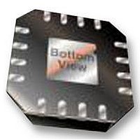
ADL5605ACPZ-R7 Analog Devices Inc, ADL5605ACPZ-R7 Datasheet - Page 15

ADL5605ACPZ-R7
Manufacturer Part Number
ADL5605ACPZ-R7
Description
IC RF DRIVER AMP 16-LFCSP
Manufacturer
Analog Devices Inc
Series
-r
Specifications of ADL5605ACPZ-R7
Current - Supply
307mA
Frequency
700MHz ~ 1GHz
Gain
23dB
Noise Figure
4.8dB
P1db
30.9dB
Package / Case
*
Rf Type
General Purpose
Test Frequency
943MHz
Voltage - Supply
4.75 V ~ 5.25 V
Noise Figure Typ
4.8dB
Power Dissipation Pd
2W
Supply Current
307mA
Supply Voltage Range
4.75V To 5.25V
Rf Ic Case Style
LFCSP
No. Of Pins
16
Rohs Compliant
Yes
Lead Free Status / Rohs Status
Lead free / RoHS Compliant
Other names
ADL5605ACPZ-R7TR
ACPR AND EVM
All adjacent channel power ratio (ACPR) and error vector
magnitude (EVM) measurements were made using a single
W-CDMA carrier and Test Model 1-64.
The signal is generated by a very low ACPR source and is meas-
ured at the output by a high dynamic range spectrum analyzer.
For ACPR measurements, the filter setting was chosen for low
ACPR; for EVM measurements, the low EVM setting was selected.
The spectrum analyzer incorporates an instrument noise correc-
tion function, and highly linear amplifiers were used to boost
the power levels for ACPR measurements.
Figure 26 shows ACPR vs. P
up to 18 dBm, an ACPR of 51 dBc or better can be achieved
at 946 MHz.
Figure 27 shows EVM vs. P
is 0.5% for power levels up to 18 dBm at 946 MHz. The baseline
composite EVM for the signal source was approximately 0.5%.
When operated in the linear region, there is little or no contribu-
tion to EVM by the amplifier.
THERMAL CONSIDERATIONS
The
4 mm, 16-lead LFCSP. The thermal resistance from junction
to air (θ
was extracted assuming a standard 4-layer JEDEC board with
25 copper plated thermal vias. The thermal vias are filled with
conductive copper paste (AE3030 with thermal conductivity of
7.8 W/mK and thermal expansion α1 of 4 × 10
8.6 × 10
is 12.1°C/W, where the case is the exposed pad of the lead frame
package.
For the best thermal performance, it is recommended that as
many thermal vias as possible be added under the exposed pad
of the LFCSP. The thermal resistance values assume a minimum
of 25 thermal vias arranged in a 5 × 5 array with a via diameter
of 8 mils, via pad of 16 mils, and a pitch of 20 mils. The vias are
plated with copper, and the drill hole is filled with a conductive
copper paste.
ADL5605
−5
JA
/°C). The thermal resistance from junction to case (θ
) is 52.1°C/W. The thermal resistance for the product
is packaged in a thermally efficient 4 mm ×
OUT
OUT
at 946 MHz. The EVM measured
at 946 MHz. For power levels
−5
/°C and α2 of
Rev. 0 | Page 15 of 20
JC
)
For optimal performance, it is recommended that the thermal
vias be filled with a conductive paste of the equivalent thermal
conductivity specified earlier in this section; alternatively, an
external heat sink can be used to dissipate heat quickly without
affecting the die junction temperature. It is also recommended
that the ground pattern be extended above and below the device
to improve thermal efficiency (see Figure 35).
SOLDERING INFORMATION AND RECOMMENDED
PCB LAND PATTERN
Figure 35 shows the recommended land pattern for the ADL5605.
To minimize thermal impedance, the exposed paddle on the
4 mm × 4 mm LFCSP is soldered to a ground plane along with
Pin 5 to Pin 8 and Pin 13 to Pin 16. To improve thermal dissi-
pation, 25 thermal vias are arranged in a 5 × 5 array under the
exposed paddle. Areas above and below the paddle are tied with
regular vias. If multiple ground layers exist, they should be tied
together using vias. For more information about land pattern
design and layout, see the
and Manufacturing Guide for the Lead Frame Chip Scale Package
(LFCSP).
16 MIL VIA PAD
WITH 8 MIL VIA
RFIN
Figure 35. Recommended Land Pattern
AN-772 Application
16
5
13
8
Note, A Design
ADL5605
RFOUT


