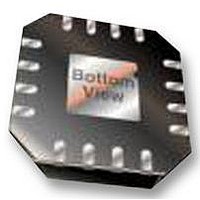
ADL5606ACPZ-R7 Analog Devices Inc, ADL5606ACPZ-R7 Datasheet

ADL5606ACPZ-R7
Specifications of ADL5606ACPZ-R7
Available stocks
Related parts for ADL5606ACPZ-R7
ADL5606ACPZ-R7 Summary of contents
Page 1
FEATURES Operation from 1800 MHz to 2700 MHz Gain of 24 2140 MHz OIP3 of 45.5 dBm at 2140 MHz P1dB of 30.8 dBm at 2140 MHz Noise figure of 4 2140 MHz Power supply: 5 ...
Page 2
ADL5606 TABLE OF CONTENTS Features .............................................................................................. 1 Applications ....................................................................................... 1 General Description ......................................................................... 1 Functional Block Diagram .............................................................. 1 Revision History ............................................................................... 2 Specifications ..................................................................................... 3 Typical Scattering Parameters ..................................................... 4 Absolute Maximum Ratings ............................................................ 6 Thermal Resistance ...................................................................... 6 ...
Page 3
SPECIFICATIONS VCC1 = 5 V and T = 25°C, unless otherwise noted. A Table 1. Parameter OVERALL FUNCTION Frequency Range FREQUENCY = 1960 MHz ± 30 MHz Gain vs. Frequency vs. Temperature vs. Supply Output 1 dB Compression Point (P1dB) ...
Page 4
ADL5606 Parameter POWER-DOWN INTERFACE Logic Level to Enable Logic Level to Disable DISABLE Pin Current VCC1 Pin Current 1 Enable Time Disable Time POWER INTERFACE Supply Voltage Supply Current vs. Temperature 1 VCC1 is the supply to the DUT through ...
Page 5
S11 Frequency (MHz) Magnitude (dB) Angle (°) 2600 −3.14 172.86 2650 −3.14 171.24 2700 −3.12 169.74 2750 −3.14 167.93 2800 −3.16 166.21 2850 −3.15 164.65 2900 −3.15 162.67 2950 −3.15 160.86 3000 −3.14 159.03 3050 −3.13 157.22 3100 −3.08 155.39 ...
Page 6
ADL5606 ABSOLUTE MAXIMUM RATINGS Table 3. Parameter 1 Supply Voltage, VCC1 Input Power (50 Ω Impedance) Internal Power Dissipation (Paddle Soldered) Maximum Junction Temperature Lead Temperature (Soldering 60 sec) Operating Temperature Range Storage Temperature Range 1 VCC1 is the supply ...
Page 7
PIN CONFIGURATION AND FUNCTION DESCRIPTIONS Table 5. Pin Function Descriptions Pin No. Mnemonic Description 1 RFIN RF Input. Requires a dc blocking capacitor. 2 DISABLE Connect this pin disable the part. In the disabled state, the ...
Page 8
ADL5606 TYPICAL PERFORMANCE CHARACTERISTICS 1960 MHZ FREQUENCY TUNING BAND 50 OIP3 (dBm P1dB (dBm) 30 GAIN (dB (dB 1930 1940 1950 1960 FREQUENCY (MHz) Figure 4. Noise Figure, Gain, P1dB, ...
Page 9
MHZ FREQUENCY TUNING BAND 60 50 OIP3 (dBm) 40 P1dB (dBm) 30 GAIN (dB (dB) 0 2110 2120 2130 2140 FREQUENCY (MHz) Figure 10. Noise Figure, Gain, P1dB, and OIP3 vs. Frequency (OIP3 ...
Page 10
ADL5606 2630 MHZ FREQUENCY TUNING BAND 60 50 OIP3 (dBm) 40 P1dB (dBm) 30 GAIN (dB (dB) 0 2570 2590 2610 2630 FREQUENCY (MHz) Figure 16. Noise Figure, Gain, P1dB, and OIP3 vs. Frequency (OIP3 at P ...
Page 11
GENERAL 43.0 43.5 44.0 44.5 45.0 45.5 OIP3 (dBm) Figure 22. OIP3 Distribution at 2140 MHz, 14 dBm per Tone 29.8 30.0 30.2 30.4 ...
Page 12
ADL5606 375 5.25V 370 5V 365 4.75V 360 355 350 345 340 –40 – TEMPERATURE (°C) Figure 28. Supply Current vs. Temperature and Supply Voltage at 2140 MHz 3 2 CH2 1V Ω M20ns 10GS/s CH3 1V ...
Page 13
APPLICATIONS INFORMATION BASIC LAYOUT CONNECTIONS The basic connections for operating the in Figure 31. The RF matching components correspond to the 2140 MHz frequency tuning band. Power Supply The voltage supply for the ADL5606, which ranges from 4. ...
Page 14
ADL5606 ADL5606 MATCHING The RF input and output of the ADL5606 to 50 Ω with at most one external component and the micro- strip line used as an inductor. Table 6 lists the required matching component values. Capacitors C and ...
Page 15
ACPR AND EVM All adjacent channel power ratio (ACPR) and error vector magnitude (EVM) measurements were made using a single W-CDMA carrier and Test Model 1-64. The signal is generated by a very low ACPR source and is meas- ured ...
Page 16
ADL5606 EVALUATION BOARD The schematic of the ADL5606 evaluation board is shown in Figure 36. The evaluation board uses 25 mils wide, 50 Ω traces and is made from IS410 material with a 20 mils gap to ground. The evaluation ...
Page 17
Figure 37. Evaluation Board Layout, Top Figure 38. Evaluation Board Layout, Bottom Rev Page ADL5606 ...
Page 18
... INDICATOR TOP VIEW 12° MAX 1.00 0.85 0.80 SEATING PLANE COMPLIANT TO JEDEC STANDARDS MO-220-VGGC ORDERING GUIDE 1 Model Temperature Range ADL5606ACPZ-R7 −40°C to +85°C ADL5606-EVALZ RoHS Compliant Part. 0.60 MAX 0.60 MAX 13 12 0.65 BSC EXPOSED 3.75 BSC SQ (BOTTOM VIEW) 0. ...
Page 19
NOTES Rev Page ADL5606 ...
Page 20
ADL5606 NOTES ©2011 Analog Devices, Inc. All rights reserved. Trademarks and registered trademarks are the property of their respective owners. D09968-0-7/11(0) Rev Page ...


