MP34DB01TR STMicroelectronics, MP34DB01TR Datasheet
MP34DB01TR
Specifications of MP34DB01TR
Available stocks


Related parts for MP34DB01TR


MP34DB01TR Summary of contents
Page 1
... IC interface with stereo operation capability. Table 1. Device summary Part number Temperature range [°C] MP34DB01 MP34DB01TR April 2011 This is preliminary information on a new product now in development or undergoing evaluation. Details are subject to change without notice. omnidirectional digital microphone The sensing element, capable of detecting ...
Page 2
Contents Contents 1 Pin descriptions . . . . . . . . . . . . . . . . . . . . . . . . . . . . . . . . . . . ...
Page 3
MP34DB01 List of tables Table 2. Pin descriptions . . . . . . . . . . . . . . . . . . . . . . . . . . . . . . . . ...
Page 4
List of figures List of figures Figure 1. Pin connections . . . . . . . . . . . . . . . . . . . . . . . . . . . . . . ...
Page 5
MP34DB01 1 Pin descriptions Figure 1. Pin connections Table 2. Pin descriptions Pin # Pin name CLK Synchronization input clock LR Left/right channel selection Vdd Power supply DOUT Left/right PDM data output GND 0 V ...
Page 6
Acoustic and electrical specifications 2 Acoustic and electrical specifications 2.1 Acoustic and electrical characteristics The values listed in the table below are specified for Vdd = 1.8 V, Clock = 2.4 MHz °C, unless otherwise noted. Table ...
Page 7
MP34DB01 2.2 Timing characteristics Table 5. Timing characteristics Parameter f Clock frequency for normal mode CLK f Clock frequency for power-down mode PD T Clock period for normal mode CLK T Data enabled on DATA line, L/R pin = 1 ...
Page 8
Acoustic and electrical specifications 2.3 Frequency response Figure 3. Typical frequency response normalized at 1 kHz Table 6. Frequency response mask for digital microphones Frequency / Hz 20...100 100...8000 8000...20000 °C and acoustic stimulus = ...
Page 9
MP34DB01 3 Absolute maximum ratings Stresses above those listed as “absolute maximum ratings” may cause permanent damage to the device. This is a stress rating only and functional operation of the device under these conditions is not implied. Exposure to ...
Page 10
Functionality 4 Functionality 4.1 L/R channel selection The L/R digital pad lets the user select the DOUT signal pattern as explained in L/R pin must be connected to Vdd or GND. Table 8. L/R channel selection L/R GND Vdd 10/16 ...
Page 11
MP34DB01 5 Application recommendations Figure 4. MP34DB01 electrical connections Figure 5. MP34DB01 electrical connections for stereo configuration Power supply decoupling capacitors (100 nF ceramic, 10 µF ceramic) should be placed as near as possible to pin 3 of the device ...
Page 12
Package mechanical data 6 Package mechanical data In order to meet environmental requirements, ST offers these devices in different grades of ® ECOPACK packages, depending on their level of environmental compliance. ECOPACK specifications, grade definitions and product status are available ...
Page 13
MP34DB01 Figure 6. Recommended soldering profile limits SMAX T SMIN PREHEAT Table 9. Recommended soldering profile limits Description Average ramp rate Preheat Minimum temperature Maximum temperature Time ( SMIN Ramp-up ...
Page 14
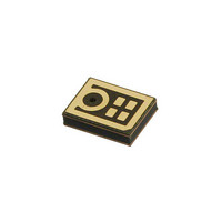
Package mechanical data Figure 7. RHLGA 4-lead package outline Bottom Port Indicator TOP VIEW Table 10. RHLGA 4-lead package dimensions Symbol ...
Page 15
MP34DB01 7 Revision history Table 11. Document revision history Date 28-Mar-2011 05-Apr-2011 Revision 1 Initial release. 2 Updated Table 3 and Doc ID 17924 Rev 2 Revision history Changes Table 5. 15/16 ...
Page 16
... Information in this document is provided solely in connection with ST products. STMicroelectronics NV and its subsidiaries (“ST”) reserve the right to make changes, corrections, modifications or improvements, to this document, and the products and services described herein at any time, without notice. All ST products are sold pursuant to ST’s terms and conditions of sale. ...