CLC011BCQ National Semiconductor, CLC011BCQ Datasheet
CLC011BCQ
Specifications of CLC011BCQ
Available stocks


Related parts for CLC011BCQ

CLC011BCQ Summary of contents
Page 1
... The CMOS compatible outputs, Block Diagram © 2002 National Semiconductor Corporation which feature controlled rise and fall times, may be set for either 3. swings with the VDP and VCP inputs. ...
Page 2
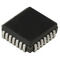
... PD0–9 17, Parallel data outputs. 19–25, 27, 28 VDP 18 Parallel data high level programming pin. The voltage at this supply pin defines the logic high level for the data outputs. www.national.com 10008602 28-Pin PLCC Order Number CLC011BCQ See NS Package Number V28A Description 2 ...
Page 3
... Absolute Maximum Ratings If Military/Aerospace specified devices are required, please contact the National Semiconductor Sales Office/ Distributors for availability and specifications. Supply Voltage (V – Storage Temperature Range Junction Temperature ESD Rating (HBM) PDx other Package Thermal Resistance θ 28-Pin PLCC JA Electrical Characteristics ...
Page 4
Electrical Characteristics Note 2: Min/Max ratings are based on product characterization and simulation. Individual parameters are tested as noted. Outgoing quality levels are determined from tested parameters. Note 3: Nominal position of rising edge of serial clock is at the ...
Page 5
Overview The CLC011, Serial Digital Video Decoder, decodes and descrambles SMPTE 259M standard Serial Digital Video datastreams into 10-bit parallel words and a corresponding word-rate clock. The following information describes: • the CLC011 operation, • recommended interface circuitry, and • ...
Page 6
Input Interfacing—Control Inputs (Continued) and a TRS, out of phase with the current PCLK, is received, output NSP will go high. However, the phase of PCLK will not be adjusted. NSP will remain high until a TRS, in-phase with the ...
Page 7
Output Interface—Control Outputs PCLK (Parallel Clock): The parallel output or word clock, PCLK, is synchronous with the parallel data outputs, PD0–9. The rising edge of PCLK is located at the center of the parallel data window. TRS (Timing Reference Signal): ...
Page 8
... National does not assume any responsibility for use of any circuitry described, no circuit patent licenses are implied and National reserves the right at any time without notice to change said circuitry and specifications. inches (millimeters) Order Number CLC011BCQ NS Package Number V28A 2. A critical component is any component of a life ...