AD743JN Analog Devices Inc, AD743JN Datasheet
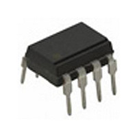
AD743JN

Manufacturer Part Number
AD743JN
Description
Manufacturer
Analog Devices Inc
Type
General Purpose Amplifierr
Datasheet

Specifications of AD743JN

Rail/rail I/o Type
No
Number Of Elements
1
Unity Gain Bandwidth Product
4.5MHz
Slew Rate
2.8V/us
Common Mode Rejection Ratio
80dB
Input Offset Voltage
1mV
Input Bias Current
200pA
Single Supply Voltage (typ)
Not RequiredV
Dual Supply Voltage (typ)
±15V
Voltage Gain In Db
132.04dB
Power Supply Rejection Ratio
90dB
Power Supply Requirement
Dual
Shut Down Feature
No
Single Supply Voltage (min)
Not RequiredV
Single Supply Voltage (max)
Not RequiredV
Dual Supply Voltage (min)
±4.8V
Dual Supply Voltage (max)
±18V
Technology
BiFET
Operating Temp Range
0C to 70C
Operating Temperature Classification
Commercial
Mounting
Through Hole
Pin Count
8
Package Type
PDIP
Lead Free Status / Rohs Status
Not Compliant

Available stocks

Company
Part Number
Manufacturer
Quantity
Price
Part Number:
AD743JN
Manufacturer:
AD
Quantity:
1 980
GENERAL DESCRIPTION
The AD743 is an ultralow noise, precision, FET input, monolithic
operational amplifier. It offers a combination of the ultralow volt-
age noise generally associated with bipolar input op amps and
the very low input current of a FET input device. Furthermore,
the AD743 does not exhibit an output phase reversal when the
negative common-mode voltage limit is exceeded.
The AD743’s guaranteed, maximum input voltage noise of
4.0 nV/√Hz at 10 kHz is unsurpassed for a FET input mono-
lithic op amp, as is the maximum 1.0 µV p-p, 0.1 Hz to 10 Hz
noise. The AD743 also has excellent dc performance with 250 pA
maximum input bias current and 0.5 mV maximum offset voltage.
The AD743 is specifically designed for use as a preamp in capaci-
tive sensors, such as ceramic hydrophones. The AD743J is rated
over the commercial temperature range of 0°C to 70°C.
The AD743 is available in a 16-lead SOIC and 8-lead PDIP.
PRODUCT HIGHLIGHTS
1. The low offset voltage and low input offset voltage drift of the
REV. E
Information furnished by Analog Devices is believed to be accurate and
reliable. However, no responsibility is assumed by Analog Devices for its
use, nor for any infringements of patents or other rights of third parties that
may result from its use. No license is granted by implication or otherwise
under any patent or patent rights of Analog Devices. Trademarks and
registered trademarks are the property of their respective companies.
FEATURES
Ultralow Noise Performance
Excellent DC Performance
AC Performance
APPLICATIONS
Sonar Preamplifiers
High Dynamic Range Filters (>140 dB)
Photodiode and IR Detector Amplifiers
Accelerometers
AD743 coupled with its ultralow noise performance mean
that the AD743 can be used for upgrading many applications
now using bipolar amplifiers.
2.9 nV/
0.38 V p-p, 0.1 Hz to 10 Hz
6.9 fA/
0.5 mV Max Offset Voltage
250 pA Max Input Bias Current
1000 V/mV Min Open-Loop Gain
2.8 V/ s Slew Rate
4.5 MHz Unity-Gain Bandwidth
THD = 0.0003% @ 1 kHz
Available in Tape and Reel in Accordance with
EIA-481A Standard
Hz Current Noise at 1 kHz
Hz at 10 kHz
2. The combination of low voltage and low current noise make
3. The low input offset voltage and low noise level of the AD743
4. The typical 10 kHz noise level of 2.9 nV/√Hz permits a three
One Technology Way, P.O. Box 9106, Norwood, MA 02062-9106, U.S.A.
Tel: 781/329-4700
Fax: 781/326-8703
NULL
–V
+IN
–IN
the AD743 ideal for charge sensitive applications such as
accelerometers and hydrophones.
provide >140 dB dynamic range.
op amp instrumentation amplifier, using three AD743s, to be
built which exhibits less than 4.2 nV/√Hz noise at 10 kHz
and which has low input bias currents.
Figure 1. Input Voltage Noise vs. Source Resistance
S
8-Lead PDIP (N)
1
2
3
4
NC = NO CONNECT
1000
TOP VIEW
100
AD743
10
1
100
AD743 AND RESISTOR
OP27 AND RESISTOR
CONNECTION DIAGRAMS
R
R
SOURCE
SOURCE
© 2003 Analog Devices, Inc. All rights reserved.
1k
8
8
7
6
5
RESISTOR NOISE ONLY
OR
SOURCE RESISTANCE ( )
NC
OUT
NULL
+V
S
E
O
(– – –)
10k
OFFSET
NULL
–V
Ultralow Noise
–IN
+IN
NC
NC
NC
NC
OP27 AND
RESISTOR
BiFET Op Amp
S
100k
( — )
16-Lead SOIC (R)
1
2
3
4
6
7
8
5
NC = NO CONNECT
AD743 AND
RESISTOR
TOP VIEW
(
AD743
1M
AD743
)
www.analog.com
10M
16
15
14
13
12
11
10
8
9
NC
NC
NC
OUTPUT
NC
NC
+V
OFFSET
NULL
S

Related parts for AD743JN

AD743JN Summary of contents

Page 1

FEATURES Ultralow Noise Performance √ kHz 2.9 nV/ 0.38 V p-p, 0 √ Hz Current Noise at 1 kHz 6.9 fA/ Excellent DC Performance 0.5 mV Max Offset Voltage 250 pA Max Input ...

Page 2

AD743–SPECIFICATIONS Parameter 1 INPUT OFFSET VOLTAGE Initial Offset Initial Offset vs. Temperature vs. Supply (PSRR) vs. Supply (PSRR) 3 INPUT BIAS CURRENT Either Input Either Input @ T MAX Either Input = ± Either Input INPUT ...

Page 3

... Although the AD743 features proprietary ESD protection circuitry, permanent damage may occur on devices subjected to high energy electrostatic discharges. Therefore, proper ESD precautions are recommended to avoid performance degradation or loss of functionality. REV. E ORDERING GUIDE Model S AD743JN and –V AD743JR- AD743JR-16-REEL AD743JR-16-REEL7 *N = PDIP SOIC. ...

Page 4

AD743–Typical Performance Characteristics (@ 10k LOAD – SUPPLY VOLTAGE ( V) TPC 1. Input Voltage Swing vs. Supply Voltage ...

Page 5

PHASE GAIN –20 –20 100 1k 10k 100k 1M 10M 100M FREQUENCY (Hz) TPC 10. Open-Loop Gain and Phase vs. Frequency 120 100 V = 10V CM 80 ...

Page 6

AD743 2.5 2.7 2.9 3.1 INPUT VOLTAGE NOISE (nV/ Hz) TPC 19. Typical Noise Distribution @ 10 kHz (602 Units 0 ...

Page 7

OP AMP PERFORMANCE: JFET VS. BIPOLAR The AD743 is the first monolithic JFET op amp to offer the low input voltage noise of an industry-standard bipolar op amp without its inherent input current errors. This is demonstrated in Figure 2, ...

Page 8

AD743 Figures 4 and 5 show two ways to buffer and amplify the output of a charge output transducer. Both require using an amplifier that has a very high input impedance, such as the AD743. Figure 4 shows a model ...

Page 9

HOW CHIP PACKAGE TYPE AND POWER DISSIPATION AFFECT INPUT BIAS CURRENT As with all JFET input amplifiers, the input bias current of the AD743 is a direct function of device junction temperature, I approximately doubling every 10°C. Figure 8 shows ...

Page 10

AD743 AN INPUT IMPEDANCE COMPENSATED, SALLEN-KEY FILTER The simple high-pass filter of Figure 13 has an important source of error which is often overlooked. Even input capacitance in amplifier A will contribute an additional 1% of pass-band ...

Page 11

R2 1900 R3 100 C1* R4 AD743 B AND K TYPE 8100 HYDROPHONE INPUT SENSITIVITY = –179 dB re. 1V/ Pa** *OPTIONAL, SEE TEXT **1V PER MICROPASCAL Figure 15b. AC-Coupled, Low Noise Hydrophone ...

Page 12

AD743 8-Lead Plastic Dual In-Line Package [PDIP] (N-8) Dimensions shown in inches and (millimeters) 0.375 (9.53) 0.365 (9.27) 0.355 (9.02 0.295 (7.49) 0.285 (7.24) 0.275 (6.98 0.100 (2.54) BSC 0.015 0.180 (0.38) (4.57) MIN MAX 0.150 ...

Related keywords