MC14174B
Hex Type D Flip−Flop
P−channel and N−channel enhancement mode devices in a single
monolithic structure. Data on the D inputs which meets the setup time
requirements is transferred to the Q outputs on the positive edge of the
clock pulse. All six flip−flops share common clock and reset inputs.
The reset is active low, and independent of the clock.
Features
•
•
•
•
•
•
•
Stresses exceeding Maximum Ratings may damage the device. Maximum
Ratings are stress ratings only. Functional operation above the Recommended
Operating Conditions is not implied. Extended exposure to stresses above the
Recommended Operating Conditions may affect device reliability.
1. Temperature Derating: Plastic “P and D/DW”
static voltages or electric fields. However, precautions must be taken to avoid
applications of any voltage higher than maximum rated voltages to this
high−impedance circuit. For proper operation, V
to the range V
(e.g., either V
*For additional information on our Pb−Free strategy and soldering details, please
MAXIMUM RATINGS
© Semiconductor Components Industries, LLC, 2006
June, 2006 − Rev. 6
DC Supply Voltage Range
Input or Output Voltage Range
(DC or Transient)
Input or Output Current (DC or Transient)
per Pin
Power Dissipation, per Package (Note 1)
Ambient Temperature Range
Storage Temperature Range
Lead Temperature (8−Second Soldering)
download the ON Semiconductor Soldering and Mounting Techniques
Reference Manual, SOLDERRM/D.
The MC14174B hex type D flip−flop is constructed with MOS
This device contains protection circuitry to guard against damage due to high
Unused inputs must always be tied to an appropriate logic voltage level
Schottky TTL Load Over the Rated Temperature Range
Static Operation
All Inputs and Outputs Buffered
Diode Protection on All Inputs
Supply Voltage Range = 3.0 Vdc to 18 Vdc
Capable of Driving Two Low−Power TTL Loads or One Low−Power
Functional Equivalent to TTL 74174
Pb−Free Packages are Available*
Packages: – 7.0 mW/_C From 65_C To 125_C
SS
SS
Parameter
or V
v (V
DD
in
). Unused outputs must be left open.
or V
(Voltages Referenced to V
out
) v V
DD
.
Symbol
V
I
in
in
in
V
P
T
, V
, I
and V
DD
D
A
out
out
SS
out
)
−0.5 to +18.0
−55 to +125
−65 to +150
−0.5 to V
should be constrained
Value
+ 0.5
± 10
500
260
DD
1
Unit
mW
mA
°C
°C
°C
V
V
†For information on tape and reel specifications,
MC14174BCP
MC14174BCPG
MC14174BD
MC14174BDG
MC14174BDR2
MC14174BDR2G
including part orientation and tape sizes, please
refer to our Tape and Reel Packaging Specifications
Brochure, BRD8011/D.
1
1
Device
ORDERING INFORMATION
A
WL
YY, Y = Year
WW
G
http://onsemi.com
CASE 751B
= Assembly Location
= Wafer Lot
= Work Week
= Pb−Free Package
CASE 648
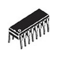
P SUFFIX
D SUFFIX
SOIC−16
PDIP−16
(Pb−Free)
(Pb−Free)
(Pb−Free)
SOIC−16
SOIC−16
SOIC−16
SOIC−16
Package
PDIP−16
PDIP−16
Publication Order Number:
16
16
1
1
2500/Tape & Reel
2500/Tape & Reel
25 Units/Rail
25 Units/Rail
DIAGRAMS
MC14174BCP
48 Units/Rail
48 Units/Rail
AWLYYWWG
Shipping
MARKING
AWLYWW
14174BG
MC14174B/D
†