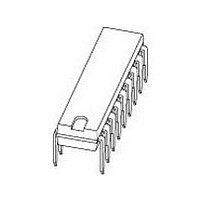
TDA1517P NXP Semiconductors, TDA1517P Datasheet - Page 7

TDA1517P
Manufacturer Part Number
TDA1517P
Description
Manufacturer
NXP Semiconductors
Datasheet
1.TDA1517P.pdf
(15 pages)
Specifications of TDA1517P
Operational Class
Class-B
Audio Amplifier Output Configuration
2-Channel Stereo
Output Power (typ)
6x2@4OhmW
Audio Amplifier Function
Speaker
Total Harmonic Distortion
0.1@4Ohm@1W%
Single Supply Voltage (typ)
14.4V
Dual Supply Voltage (typ)
Not RequiredV
Power Supply Requirement
Single
Power Dissipation
15W
Rail/rail I/o Type
No
Power Supply Rejection Ratio
80dB
Single Supply Voltage (min)
6V
Single Supply Voltage (max)
18V
Dual Supply Voltage (min)
Not RequiredV
Dual Supply Voltage (max)
Not RequiredV
Operating Temp Range
-40C to 85C
Operating Temperature Classification
Industrial
Mounting
Through Hole
Pin Count
18
Package Type
HDIP
Lead Free Status / Rohs Status
Compliant
Available stocks
Company
Part Number
Manufacturer
Quantity
Price
Company:
Part Number:
TDA1517P
Manufacturer:
PHILIPS
Quantity:
505
Part Number:
TDA1517P
Manufacturer:
NXP/恩智浦
Quantity:
20 000
Company:
Part Number:
TDA1517P/N3
Manufacturer:
NXP Semiconductors
Quantity:
1 966
Company:
Part Number:
TDA1517P/N3
Manufacturer:
NXP
Quantity:
20 000
Company:
Part Number:
TDA1517PN3
Manufacturer:
ON
Quantity:
7 272
NXP Semiconductors
AC CHARACTERISTICS
V
Notes
1. Output power is measured directly at the output pins of the IC.
2. Frequency response externally fixed.
3. Ripple rejection measured at the output with a source impedance of 0 Ω, maximum ripple amplitude of 2 V (p-p) and
4. Noise voltage measured in a bandwidth of 20 Hz to 20 kHz.
5. Noise output voltage independent of R
2004 Feb 18
P
THD
f
f
G
SVRR
|Z
V
α
|ΔG
P
lr
hr
cs
o
no
2 x 6 W stereo power amplifier
v
i
|
= 14.4 V; R
a frequency between 100 Hz and 10 kHz.
SYMBOL
v
|
L
= 4 Ω; f = 1 kHz; T
output power
total harmonic distortion
low frequency roll-off
high frequency roll-off
closed loop voltage gain
supply voltage ripple rejection
input impedance
noise output voltage
channel separation
channel unbalance
on
mute
standby
on
on
mute
PARAMETER
amb
= 25 °C; measured in Fig.6; unless otherwise specified.
s
(V
I
= 0 V).
THD = 0.5%; note 1
THD = 10%; note 1
P
at −3 dB; note 2
at −1 dB
note 3
R
R
note 5
R
o
s
s
s
= 1 W
= 0 Ω; note 4
= 10 Ω; note 4
= 10 Ω
CONDITIONS
7
4
5.5
−
−
20
19
48
48
80
50
−
−
−
40
−
MIN.
TDA1517; TDA1517P
5
6.0
0.1
45
−
20
−
−
−
60
50
70
50
−
0.1
TYP.
Product specification
−
−
−
−
−
21
−
−
−
75
−
100
−
−
1
MAX.
W
W
%
Hz
kHz
dB
dB
dB
dB
kΩ
μV
μV
μV
dB
dB
UNIT


