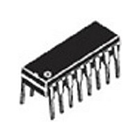
MC14543B
BCD−to−Seven Segment
Latch/Decoder/Driver for
Liquid Crystals
designed for use with liquid crystal readouts, and is constructed with
complementary MOS (CMOS) enhancement mode devices. The
circuit provides the functions of a 4−bit storage latch and an 8421
BCD−to−seven segment decoder and driver. The device has the
capability to invert the logic levels of the output combination. The
phase (Ph), blanking (BI), and latch disable (LD) inputs are used to
reverse the truth table phase, blank the display, and store a BCD code,
respectively. For liquid crystal (LC) readouts, a square wave is applied
to the Ph input of the circuit and the electrically common backplane of
the display. The outputs of the circuit are connected directly to the
segments of the LC readout. For other types of readouts, such as
light−emitting diode (LED), incandescent, gas discharge, and
fluorescent readouts, connection diagrams are given on this data sheet.
driver, computer/calculator display driver, cockpit display driver, and
various clock, watch, and timer uses.
Features
•
•
•
•
•
•
•
•
•
Stresses exceeding Maximum Ratings may damage the device. Maximum
Ratings are stress ratings only. Functional operation above the Recommended
Operating Conditions is not implied. Extended exposure to stresses above the
Recommended Operating Conditions may affect device reliability.
1. Temperature Derating: Plastic “P and D/DW”
2. P
MAXIMUM RATINGS
© Semiconductor Components Industries, LLC, 2006
June, 2006 − Rev. 6
DC Supply Voltage Range
Input Voltage Range, All Inputs
DC Input Current per Pin
Power Dissipation per Package (Note 1)
Operating Temperature Range
Storage Temperature Range
Maximum Continuous Output Drive
Current (Source or Sink)
Maximum Continuous Output Power
(Source or Sink) (Note 2)
The MC14543B BCD−to−seven segment latch/decoder/driver is
Applications include instrument (e.g., counter, DVM etc.) display
TTL Load or 2 HTL Loads Over the Rated Temperature Range
Latch Storage of Code
Blanking Input
Readout Blanking on All Illegal Input Combinations
Direct LED (Common Anode or Cathode) Driving Capability
Supply Voltage Range = 3.0 V to 18 V
Capable of Driving 2 Low−power TTL Loads, 1 Low−power Schottky
Pin−for−Pin Replacement for CD4056A (with Pin 7 Tied to V
Chip Complexity: 207 FETs or 52 Equivalent Gates
Pb−Free Packages are Available*
Packages: – 7.0 mW/_C From 65_C To 125_C
OHmax
= I
OH
Parameter
(V
OH
− V
(Voltages Referenced to V
DD
) and P
OLmax
Symbol
P
P
= I
I
I
OHmax
OLmax
OHmax
OLmax
V
T
V
P
T
I
OL
DD
stg
in
in
A
D
(V
OL
SS
−0.5 to V
)
− V
−0.5 to +18.0
−55 to +125
−65 to +150
(per Output)
(per Output)
SS
Value
± 10
500
10
70
)
DD
+0.5
1
Unit
mW
mW
mA
mA
SS
°C
°C
V
V
).
against damage due to high static voltages or electric
fields. However, precautions must be taken to avoid
applications of any voltage higher than maximum rated
voltages to this high−impedance circuit. For proper
operation, V
range V
logic voltage level (e.g., either V
outputs must be left open.
See detailed ordering and shipping information in the package
dimensions section on page 2 of this data sheet.
*For additional information on our Pb−Free strategy
and soldering details, please download the
ON Semiconductor Soldering and Mounting
Techniques Reference Manual, SOLDERRM/D.
1
This device contains protection circuitry to guard
Unused inputs must always be tied to an appropriate
1
1
SS
ORDERING INFORMATION
v (V
A
WL, L
YY, Y
WW, W = Work Week
G
in
and V
http://onsemi.com
in
or V
CASE 751B
SOEIAJ−16
CASE 648
CASE 966
D SUFFIX
P SUFFIX
F SUFFIX
PDIP−16
SOIC−16
= Assembly Location
= Wafer Lot
= Year
= Pb−Free Package
out
out
should be constrained to the
) v V
Publication Order Number:
DD
16
16
16
1
1
1
.
SS
or V
MC14543BCP
DIAGRAMS
AWLYYWWG
MARKING
MC14543B
AWLYWW
14543BG
MC14543B/D
ALYWG
DD
). Unused


