HEF4511BP NXP Semiconductors, HEF4511BP Datasheet
HEF4511BP
Specifications of HEF4511BP
Available stocks


Related parts for HEF4511BP


HEF4511BP Summary of contents
Page 1
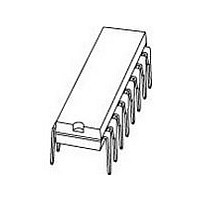
... Ordering information − ° All types operate from +125 Type number Package Name Description HEF4511BP DIP16 plastic dual in-line package; 16 leads (300 mil) HEF4511BT SO16 plastic small outline package; 16 leads; body width 3.9 mm power supply range referenced ° C. Product data sheet ...
Page 2
... NXP Semiconductors 5. Functional diagram Fig 1. Functional diagram Fig 2. Schematic diagram of output stage HEF4511B_6 Product data sheet LATCHES BL DECODER LT DRIVERS driver logic 001aae677 Rev. 06 — 7 December 2009 HEF4511B BCD to 7-segment latch/decoder/driver 001aae675 + V OH − © NXP B.V. 2009. All rights reserved ...
Page 3
latch Fig 3. Logic diagram latch latch ...
Page 4
... NXP Semiconductors 6. Pinning information 6.1 Pinning Fig 4. Pin configuration DIP16 and SO16 6.2 Pin description Table 2. Pin description Symbol Pin 13, 12, 11, 10 HEF4511B_6 Product data sheet BCD to 7-segment latch/decoder/driver HEF4511B 001aae676 Description lamp test input (active LOW) ripple blanking input (active LOW) ...
Page 5
... NXP Semiconductors 7. Functional description [1] Table 3. Function table Inputs [ HIGH voltage level LOW voltage level don’t care; N. change. Fig 5. Seven segment digital display with segment designation HEF4511B_6 Product data sheet Outputs N.C. N.C. N.C. Rev. 06 — 7 December 2009 HEF4511B BCD to 7-segment latch/decoder/driver ...
Page 6
... NXP Semiconductors 8. Limiting values Table 4. Limiting values In accordance with the Absolute Maximum Rating System (IEC 60134). Symbol Parameter V supply voltage DD I input clamping current IK V input voltage I I output clamping current OK I input/output current I/O I HIGH-level output current OH I supply current ...
Page 7
... NXP Semiconductors 10. Static characteristics Table 6. Static characteristics unless otherwise specified Symbol Parameter Conditions < 1 μA V HIGH-level IH O input voltage |I | < 1 μA V LOW-level IL O input voltage V HIGH-level see Table 7 OH output voltage |I | < 1 μA V LOW-level OL O output voltage I HIGH-level output current ...
Page 8
... NXP Semiconductors Table 7. Static characteristics for Symbol Parameter HIGH-level 0 OH output voltage 11. Dynamic characteristics Table 8. Dynamic characteristics ° for test circuit see SS amb Symbol Parameter Conditions Dn → Qn; t HIGH to LOW PHL propagation delay see LE → Qn; see BL → Qn; see LT → Qn; see HEF4511B_6 ...
Page 9
... NXP Semiconductors Table 8. Dynamic characteristics ° for test circuit see SS amb Symbol Parameter Conditions Dn → Qn; t LOW to HIGH PLH propagation delay see LE → Qn; see BL → Qn; see LT → Qn; see t HIGH to LOW output see THL transition time t LOW to HIGH output see TLH transition time Dn → ...
Page 10
... NXP Semiconductors 12. Waveforms PLH t PHL THL TLH Conditions LOW and HIGH. Measurement points are given in Fig 6. Propagation delays and output transition times HEF4511B_6 Product data sheet PLH t PHL Table 10. Rev. 06 — 7 December 2009 HEF4511B BCD to 7-segment latch/decoder/driver PLH PLH t PHL © NXP B.V. 2009. All rights reserved. ...
Page 11
... NXP Semiconductors LE input V D2 input output V The shaded area indicates where the input is permitted to change for predictable output performance. Conditions LOW and HIGH. Measurement points are given in Fig 7. Waveforms showing minimum LE pulse width, set-up, and hold time for HEF4511B_6 Product data sheet ...
Page 12
... NXP Semiconductors negative positive a. Input waveforms b. Test circuit Test data is given in Table 10. Definitions for test circuit: DUT = Device Under Test Load capacitance including jig and probe capacitance Termination resistance should be equal to output impedance Z T Fig 8. Test circuit for measuring switching times Table 10 ...
Page 13
... NXP Semiconductors 13. Application information • Driving LED displays • Driving incandescent displays • Driving fluorescent displays • Driving LCD displays • Driving gas discharge displays Fig 9. Connection to common cathode LED display readout (1) A filament pre-warm resistor is recommended to reduce filament thermal shock and increase the effective cold resistance of the filament ...
Page 14
... NXP Semiconductors Fig 13. Connection to gas discharge display readout HEF4511B_6 Product data sheet appropriate voltage 001aae687 Direct DC drive of LCDs not recommended for life of LCD readouts. Fig 14. Connection to LCD readout Rev. 06 — 7 December 2009 HEF4511B BCD to 7-segment latch/decoder/driver exitation V DD (square wave DD) ...
Page 15
... NXP Semiconductors 14. Package outline DIP16: plastic dual in-line package; 16 leads (300 mil pin 1 index 1 DIMENSIONS (inch dimensions are derived from the original mm dimensions UNIT b max. min. max. 1.73 mm 4.2 0.51 3.2 1.30 0.068 inches 0.17 0.02 0.13 0.051 Note 1. Plastic or metal protrusions of 0.25 mm (0.01 inch) maximum per side are not included. ...
Page 16
... NXP Semiconductors SO16: plastic small outline package; 16 leads; body width 3 pin 1 index 1 e DIMENSIONS (inch dimensions are derived from the original mm dimensions) A UNIT max. 0.25 1.45 mm 1.75 0.25 0.10 1.25 0.010 0.057 inches 0.069 0.01 0.004 0.049 Note 1. Plastic or metal protrusions of 0.15 mm (0.006 inch) maximum per side are not included. ...
Page 17
... NXP Semiconductors 15. Revision history Table 11. Revision history Document ID Release date HEF4511B_6 20091207 • Modifications: Section 9 “Recommended operating HEF4511B_5 20090813 HEF4511B_4 20090305 HEF4511B_CNV_3 19950101 HEF4511B_CNV_2 19950101 HEF4511B_6 Product data sheet BCD to 7-segment latch/decoder/driver Data sheet status Change notice Product data sheet - conditions”: Δt/ΔV values updated. ...
Page 18
... Right to make changes — NXP Semiconductors reserves the right to make changes to information published in this document, including without limitation specifications and product descriptions, at any time and without notice ...
Page 19
... NXP Semiconductors 18. Contents 1 General description . . . . . . . . . . . . . . . . . . . . . . 1 2 Features . . . . . . . . . . . . . . . . . . . . . . . . . . . . . . . 1 3 Applications . . . . . . . . . . . . . . . . . . . . . . . . . . . . 1 4 Ordering information . . . . . . . . . . . . . . . . . . . . . 1 5 Functional diagram . . . . . . . . . . . . . . . . . . . . . . 2 6 Pinning information . . . . . . . . . . . . . . . . . . . . . . 4 6.1 Pinning . . . . . . . . . . . . . . . . . . . . . . . . . . . . . . . 4 6.2 Pin description . . . . . . . . . . . . . . . . . . . . . . . . . 4 7 Functional description . . . . . . . . . . . . . . . . . . . 5 8 Limiting values Recommended operating conditions Static characteristics Dynamic characteristics . . . . . . . . . . . . . . . . . . 8 12 Waveforms . . . . . . . . . . . . . . . . . . . . . . . . . . . . 10 13 Application information Package outline ...