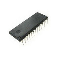
UPD43257BCZ-85L Renesas Electronics America, UPD43257BCZ-85L Datasheet

UPD43257BCZ-85L
Specifications of UPD43257BCZ-85L
Available stocks
Related parts for UPD43257BCZ-85L
UPD43257BCZ-85L Summary of contents
Page 1
Description μ The PD43257B is a high speed, low power, and 262,144 bits (32,768 words by 8 bits) CMOS static RAM. Battery backup is available. And the μ The PD43257B is packed in 28-pin PLASTIC DIP and 28-pin PLASTIC SOP. ...
Page 2
Ordering Information Part number Package μ PD43257BCZ-70L 28-pin PLASTIC DIP μ PD43257BCZ-85L (15.24 mm (600)) μ PD43257BCZ-70LL μ PD43257BCZ-85LL μ PD43257BGU-70L 28-pin PLASTIC SOP μ PD43257BGU-85L (11.43 mm (450)) μ PD43257BGU-70LL μ PD43257BGU-85LL μ PD43257BGU-70L-A 28-pin PLASTIC SOP μ PD43257BGU-85L-A ...
Page 3
Pin Configurations (Marking Side) /xxx indicates active low signal. A14 A12 I/O1 I/O2 I/O3 GND Remark Refer to Package Drawings for the 1-pin marking. 28-pin PLASTIC DIP (15.24 mm (600)) μ [ ...
Page 4
A14 A12 I/O1 I/O2 I/O3 GND Remark Refer to Package Drawings for the 1-pin marking. 4 28-pin PLASTIC SOP (11.43 mm (450)) μ [ PD43257BGU-xxL ] μ [ PD43257BGU-xxLL ] μ [ ...
Page 5
Block Diagram A0 Address buffer A14 I/O1 I/O8 /CE1 CE2 / GND Truth Table /CE1 CE2 /WE × × H × × Remark × Row ...
Page 6
Electrical Specifications Absolute Maximum Ratings Parameter Symbol Supply voltage Input / Output voltage Operating ambient temperature Storage temperature Note –3.0 V (MIN.) (Pulse width : 50 ns) Caution Exposing the device to stress above those listed in Absolute Maximum Rating ...
Page 7
DC Characteristics (Recommended Operating Conditions Unless Otherwise Noted) Parameter Symbol Input leakage current I/O leakage /CE1 = V LO I/O CC current ...
Page 8
AC Characteristics (Recommended Operating Conditions Unless Otherwise Noted) AC Test Conditions μ μ [ PD43257B-70L, PD43257B-85L, Input Waveform (Rise and Fall Time ≤ 5 ns) 2.2 V 1.5 V 0.8 V Output Waveform 1.5 V Output Load AC characteristics with ...
Page 9
Read Cycle Parameter Symbol Read cycle time Address access time /CE1 access time t CE2 access time t Output hold from address change /CE1 to output in low impedance t CE2 to output in low impedance t /CE1 to output ...
Page 10
Write Cycle Parameter Symbol Write cycle time t WC /CE1 to end of write t CW1 CE2 to end of write t CW2 Address valid to end of write t AW Address setup time t Write pulse width t WP ...
Page 11
Write Cycle Timing Chart 1 (/WE Controlled) Address (Input) /CE1 (Input) CE2 (Input) t /WE (Input) I/O (Input / Output) Indefinite data out Cautions 1. During address transition, at least one of pins /CE1, CE2, /WE should be inactivated. 2. ...
Page 12
Write Cycle Timing Chart 2 (/CE1 Controlled) Address (Input) /CE1 (Input) CE2 (Input) /WE (Input) High impedance I/O (Input) Cautions 1. During address transition, at least one of pins /CE1, CE2, /WE should be inactivated. 2. When I/O pins are ...
Page 13
Write Cycle Timing Chart 3 (CE2 Controlled) Address (Input) /CE1 (Input) CE2 (Input) /WE (Input) High impedance I/O (Input) Cautions 1. During address transition, at least one of pins /CE1, CE2, /WE should be inactivated. 2. When I/O pins are ...
Page 14
Low V Data Retention Characteristics (T CC Parameter Symbol /CE1 ≥ V Data retention V CCDR1 CE2 ≥ V supply voltage CE2 ≤ 0 CCDR2 Data retention CCDR1 CE2 ≥ V supply current V I ...
Page 15
Data Retention Timing Chart (1) /CE1 Controlled t CDR V CC 4.5 V /CE1 V (MIN (MIN.) CCDR V (MAX.) IL GND On the data retention mode by controlling /CE1, the input level of CE2 must be CE2 ...
Page 16
Package Drawings 28-PIN PLASTIC DIP (15.24 mm (600 NOTES 1. Each lead centerline is located within 0. its true position (T.P.) at maximum material condition. 2. Item "K" to ...
Page 17
PLASTIC SOP (11.43 mm (450 NOTE Each lead centerline is located within 0. its true position (T.P.) at maximum material condition ...
Page 18
Recommended Soldering Conditions Please consult with our sales offices for soldering conditions of the Types of Surface Mount Device μ PD43257BGU-xxL : 28-pin PLASTIC SOP (11.43 mm (450)) μ PD43257BGU-xxLL : 28-pin PLASTIC SOP (11.43 mm (450)) μ PD43257BGU-xxL-A : ...
Page 19
Revision History Edition/ Page Type of Date This Previous revision edition edition 9th edition/ p.1 p.1 Deletion Jun. 2006 Location (Previous edition → This edition) − Description of Version X has been deleted. Data Sheet M10693EJ9V0DS μ PD43257B Description 19 ...
Page 20
MEMO ] 20 Data Sheet M10693EJ9V0DS μ PD43257B ...
Page 21
MEMO ] Data Sheet M10693EJ9V0DS μ PD43257B 21 ...
Page 22
MEMO ] 22 Data Sheet M10693EJ9V0DS μ PD43257B ...
Page 23
NOTES FOR CMOS DEVICES 1 VOLTAGE APPLICATION WAVEFORM AT INPUT PIN Waveform distortion due to input noise or a reflected wave may cause malfunction. If the input of the CMOS device stays in the area between V malfunction. Take care ...
Page 24
The information in this document is current as of June, 2006. The information is subject to change without notice. For actual design-in, refer to the latest publications of NEC Electronics data sheets or data books, etc., for the most ...


