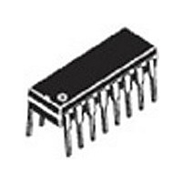
MC74HC595AN ON Semiconductor, MC74HC595AN Datasheet

MC74HC595AN
Specifications of MC74HC595AN
Available stocks
Related parts for MC74HC595AN
MC74HC595AN Summary of contents
Page 1
... Year WW Work Week Pb−Free Package (Note: Microdot may be in either location) ORDERING INFORMATION See detailed ordering and shipping information in the package dimensions section on page 2 of this data sheet. 1 MARKING DIAGRAMS 16 MC74HC595AN AWLYYWWG 1 16 HC595AG AWLYWW 595A ALYWG G 1 Publication Order Number: ...
Page 2
... RESET H GND ORDERING INFORMATION Device MC74HC595AN MC74HC595ANG MC74HC595AD MC74HC595ADG MC74HC595ADR2 MC74HC595ADR2G MC74HC595ADT MC74HC595ADTR2 MC74HC595ADTR2G MC74HC595AFEL MC74HC595AFELG †For information on tape and reel specifications, including part orientation and tape sizes, please refer to our Tape and Reel Packaging Specifications Brochure, BRD8011/D. *This package is inherently Pb−Free. ...
Page 3
... Plastic DIP: – 10 mW/_C from 65_ to 125_C SOIC Package: – 7 mW/_C from 65_ to 125_C TSSOP Package: − 6.1 mW/_C from 65_ to 125_C For high frequency or heavy load considerations, see Chapter 2 of the ON Semiconductor High−Speed CMOS Data Book (DL129/D). RECOMMENDED OPERATING CONDITIONS Î Î Î Î ...
Page 4
... Current (per Package) NOTE: Information on typical parametric values can be found in Chapter 2 of the ON Semiconductor High−Speed CMOS Data Book Î Î Î Î Î Î Î Î Î Î Î Î ...
Page 5
... C Power Dissipation Capacitance (Per Package Used to determine the no−load dynamic power consumption Semiconductor High−Speed CMOS Data Book (DL129/D). TIMING REQUIREMENTS (Input t Î Î Î Î Î Î Î Î Î Î Î Î Î Î Î Î Î Î Î Î Î ...
Page 6
Serial Input A Reset Operation Reset shift register L X Shift data into shift H D register Shift register remains H X unchanged Transfer shift register H X contents to latch register Latch register remains X X unchanged Enable parallel ...
Page 7
SHIFT 90% 50% CLOCK 10 1/f max t t PLH PHL 90% OUTPUT 50 10 TLH THL Figure 1. LATCH 50% CLOCK t t PLH PHL 90 ...
Page 8
OUTPUT 13 ENABLE LATCH 12 CLOCK SERIAL 14 DATA INPUT A SHIFT 11 CLOCK 10 RESET EXPANDED LOGIC DIAGRAM ...
Page 9
SHIFT CLOCK SERIAL DATA INPUT A RESET LATCH CLOCK OUTPUT ENABLE SERIAL DATA OUTPUT SQ H NOTE: implies that the output ...
Page 10
0.25 (0.010) −A − −B − −T − SEATING PLANE 0.25 (0.010 PACKAGE DIMENSIONS PDIP−16 ...
Page 11
... Opportunity/Affirmative Action Employer. This literature is subject to all applicable copyright laws and is not for resale in any manner. PUBLICATION ORDERING INFORMATION LITERATURE FULFILLMENT: Literature Distribution Center for ON Semiconductor P.O. Box 5163, Denver, Colorado 80217 USA Phone: 303−675−2175 or 800−344−3860 Toll Free USA/Canada Fax: 303− ...


