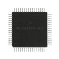
MC68HC711E9FU Freescale Semiconductor, MC68HC711E9FU Datasheet - Page 86

MC68HC711E9FU
Manufacturer Part Number
MC68HC711E9FU
Description
Manufacturer
Freescale Semiconductor
Datasheet
1.MC68HC711E9FU.pdf
(242 pages)
Specifications of MC68HC711E9FU
Cpu Family
HC11
Device Core Size
8b
Frequency (max)
4MHz
Interface Type
SCI/SPI
Program Memory Type
EPROM
Program Memory Size
12KB
Total Internal Ram Size
512Byte
# I/os (max)
38
Number Of Timers - General Purpose
8
Operating Supply Voltage (typ)
3.3/5V
Operating Supply Voltage (max)
5.5V
Operating Supply Voltage (min)
3V
On-chip Adc
8-chx8-bit
Instruction Set Architecture
CISC
Operating Temp Range
0C to 70C
Operating Temperature Classification
Commercial
Mounting
Surface Mount
Pin Count
64
Package Type
PQFP
Lead Free Status / Rohs Status
Not Compliant
Available stocks
Company
Part Number
Manufacturer
Quantity
Price
- Current page: 86 of 242
- Download datasheet (2Mb)
Resets and Interrupts
Any one of these interrupts can be assigned the highest maskable interrupt priority by writing the
appropriate value to the PSEL bits in the HPRIO register. Otherwise, the priority arrangement remains the
same. An interrupt that is assigned highest priority is still subject to global masking by the I bit in the CCR,
or by any associated local bits. Interrupt vectors are not affected by priority assignment. To avoid race
conditions, HPRIO can be written only while I-bit interrupts are inhibited.
5.4.1 Highest Priority Interrupt and Miscellaneous Register
RBOOT — Read Bootstrap ROM Bit
SMOD — Special Mode Select Bit
MDA — Mode Select A Bit
IRVNE — Internal Read Visibility/Not E Bit
PSEL[3:0] — Priority Select Bits
86
Has meaning only when the SMOD bit is a 1 (bootstrap mode or special test mode). At all other times
this bit is clear and cannot be written. Refer to
more information.
This bit reflects the inverse of the MODB input pin at the rising edge of reset. Refer to
Operating Modes and On-Chip Memory
The mode select A bit reflects the status of the MODA input pin at the rising edge of reset. Refer to
Chapter 2 Operating Modes and On-Chip Memory
The IRVNE control bit allows internal read accesses to be available on the external data bus during
operation in expanded modes. In single-chip and bootstrap modes, IRVNE determines whether the E
clock is driven out an external pin. For the MC68HC811E2, this bit is IRV and only controls internal
read visibility. Refer to
These bits select one interrupt source to be elevated above all other I-bit-related sources and can be
written only while the I bit in the CCR is set (interrupts disabled).
Reset:
1. The values of the RBOOT, SMOD, and MDA reset bits depend on the mode selected at the
Special test:
Single chip:
Expanded:
Bootstrap:
RESET pin rising edge. Refer to
Address:
Read:
Write:
RBOOT
$103C
Bit 7
Chapter 2 Operating Modes and On-Chip Memory
0
0
1
0
(1)
Figure 5-4. Highest Priority I-Bit Interrupt
SMOD
and Miscellaneous Register (HPRIO)
6
0
0
1
1
M68HC11E Family Data Sheet, Rev. 5.1
(1)
MDA
Table 2-1. Hardware Mode Select
for more information.
5
0
1
0
1
(1)
Chapter 2 Operating Modes and On-Chip Memory
IRVNE
4
0
0
0
1
for more information.
PSEL2
3
0
0
0
0
PSEL2
Summary.
2
1
1
1
1
for more information.
PSEL1
1
1
1
1
1
Freescale Semiconductor
PSEL0
Bit 0
0
0
0
0
Chapter 2
for
Related parts for MC68HC711E9FU
Image
Part Number
Description
Manufacturer
Datasheet
Request
R

Part Number:
Description:
APPENDIX A ELECTRICAL CHARACTERISTICS
Manufacturer:
FREESCALE [Freescale Semiconductor, Inc]
Datasheet:
Part Number:
Description:
Manufacturer:
Freescale Semiconductor, Inc
Datasheet:
Part Number:
Description:
Manufacturer:
Freescale Semiconductor, Inc
Datasheet:
Part Number:
Description:
Manufacturer:
Freescale Semiconductor, Inc
Datasheet:
Part Number:
Description:
Manufacturer:
Freescale Semiconductor, Inc
Datasheet:
Part Number:
Description:
Manufacturer:
Freescale Semiconductor, Inc
Datasheet:
Part Number:
Description:
Manufacturer:
Freescale Semiconductor, Inc
Datasheet:
Part Number:
Description:
Manufacturer:
Freescale Semiconductor, Inc
Datasheet:
Part Number:
Description:
Manufacturer:
Freescale Semiconductor, Inc
Datasheet:
Part Number:
Description:
Manufacturer:
Freescale Semiconductor, Inc
Datasheet:
Part Number:
Description:
Manufacturer:
Freescale Semiconductor, Inc
Datasheet:
Part Number:
Description:
Manufacturer:
Freescale Semiconductor, Inc
Datasheet:
Part Number:
Description:
Manufacturer:
Freescale Semiconductor, Inc
Datasheet:
Part Number:
Description:
Manufacturer:
Freescale Semiconductor, Inc
Datasheet:
Part Number:
Description:
Manufacturer:
Freescale Semiconductor, Inc
Datasheet:


