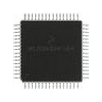
MC68HC711E9FU Freescale Semiconductor, MC68HC711E9FU Datasheet - Page 40

MC68HC711E9FU
Manufacturer Part Number
MC68HC711E9FU
Description
Manufacturer
Freescale Semiconductor
Datasheet
1.MC68HC711E9FU.pdf
(242 pages)
Specifications of MC68HC711E9FU
Cpu Family
HC11
Device Core Size
8b
Frequency (max)
4MHz
Interface Type
SCI/SPI
Program Memory Type
EPROM
Program Memory Size
12KB
Total Internal Ram Size
512Byte
# I/os (max)
38
Number Of Timers - General Purpose
8
Operating Supply Voltage (typ)
3.3/5V
Operating Supply Voltage (max)
5.5V
Operating Supply Voltage (min)
3V
On-chip Adc
8-chx8-bit
Instruction Set Architecture
CISC
Operating Temp Range
0C to 70C
Operating Temperature Classification
Commercial
Mounting
Surface Mount
Pin Count
64
Package Type
PQFP
Lead Free Status / Rohs Status
Not Compliant
Available stocks
Company
Part Number
Manufacturer
Quantity
Price
- Current page: 40 of 242
- Download datasheet (2Mb)
Operating Modes and On-Chip Memory
The bootloader program is contained in the internal bootstrap ROM. This ROM, which appears as internal
memory space at locations $BF00–$BFFF, is enabled only if the MCU is reset in special bootstrap mode.
In expanded modes, the ROM/EPROM/OTPROM (if present) is enabled out of reset and located at the
top of the memory map if the ROMON bit in the CONFIG register is set. ROM or EPROM is enabled out
of reset in single-chip and bootstrap modes, regardless of the state of ROMON.
For devices with 512 bytes of EEPROM, the EEPROM is located at $B600–$B7FF and has the same read
cycle time as the internal ROM. The 512 bytes of EEPROM cannot be remapped to other locations.
For the MC68HC811E2, EEPROM is located at $F800–$FFFF and can be remapped to any 4-Kbyte
boundary. EEPROM mapping control bits (EE[3:0] in CONFIG) determine the location of the 2048 bytes
of EEPROM and are present only on the MC68HC811E2. Refer to
for a description of the MC68HC811E2 CONFIG register.
EEPROM can be programmed or erased by software and an on-chip charge pump, allowing EEPROM
changes using the single V
2.3.2 Mode Selection
The four mode variations are selected by the logic states of the MODA and MODB pins during reset. The
MODA and MODB logic levels determine the logic state of SMOD and the MDA control bits in the highest
priority I-bit interrupt and miscellaneous (HPRIO) register.
After reset is released, the mode select pins no longer influence the MCU operating mode. In single-chip
operating mode, the MODA pin is connected to a logic level 0. In expanded mode, MODA is normally
connected to V
register LIR pin when the MCU is not in reset. The open-drain active low LIR output pin drives low during
the first E cycle of each instruction. The MODB pin also functions as standby power input (V
allows RAM contents to be maintained in absence of V
Refer to
operating modes.
40
Table
DD
2-1, which is a summary of mode pin operation, the mode control bits, and the four
through a pullup resistor of 4.7 kΩ. The MODA pin also functions as the load instruction
Figure 2-8. RAM Standby MODB/V
DD
4.8-V
NiCd
supply.
V
DD
M68HC11E Family Data Sheet, Rev. 5.1
+
V
V
DD
BATT
MAX
690
V
OUT
DD
.
4.7 k
STBY
2.3.3.1 System Configuration Register
Connections
TO MODB/V
OF M68HC11
STBY
Freescale Semiconductor
STBY
), which
Related parts for MC68HC711E9FU
Image
Part Number
Description
Manufacturer
Datasheet
Request
R

Part Number:
Description:
APPENDIX A ELECTRICAL CHARACTERISTICS
Manufacturer:
FREESCALE [Freescale Semiconductor, Inc]
Datasheet:
Part Number:
Description:
Manufacturer:
Freescale Semiconductor, Inc
Datasheet:
Part Number:
Description:
Manufacturer:
Freescale Semiconductor, Inc
Datasheet:
Part Number:
Description:
Manufacturer:
Freescale Semiconductor, Inc
Datasheet:
Part Number:
Description:
Manufacturer:
Freescale Semiconductor, Inc
Datasheet:
Part Number:
Description:
Manufacturer:
Freescale Semiconductor, Inc
Datasheet:
Part Number:
Description:
Manufacturer:
Freescale Semiconductor, Inc
Datasheet:
Part Number:
Description:
Manufacturer:
Freescale Semiconductor, Inc
Datasheet:
Part Number:
Description:
Manufacturer:
Freescale Semiconductor, Inc
Datasheet:
Part Number:
Description:
Manufacturer:
Freescale Semiconductor, Inc
Datasheet:
Part Number:
Description:
Manufacturer:
Freescale Semiconductor, Inc
Datasheet:
Part Number:
Description:
Manufacturer:
Freescale Semiconductor, Inc
Datasheet:
Part Number:
Description:
Manufacturer:
Freescale Semiconductor, Inc
Datasheet:
Part Number:
Description:
Manufacturer:
Freescale Semiconductor, Inc
Datasheet:
Part Number:
Description:
Manufacturer:
Freescale Semiconductor, Inc
Datasheet:


