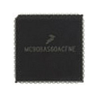
MC68HC11E1CFN3R2 Freescale Semiconductor, MC68HC11E1CFN3R2 Datasheet - Page 121

MC68HC11E1CFN3R2
Manufacturer Part Number
MC68HC11E1CFN3R2
Description
Manufacturer
Freescale Semiconductor
Datasheet
1.MC68HC11E1CFN3R2.pdf
(242 pages)
Specifications of MC68HC11E1CFN3R2
Cpu Family
HC11
Device Core Size
8b
Frequency (max)
3MHz
Interface Type
SCI/SPI
Program Memory Type
ROMLess
Program Memory Size
Not Required
Total Internal Ram Size
512Byte
# I/os (max)
38
Number Of Timers - General Purpose
8
Operating Supply Voltage (typ)
3.3/5V
Operating Supply Voltage (max)
5.5V
Operating Supply Voltage (min)
3V
On-chip Adc
8-chx8-bit
Instruction Set Architecture
CISC
Operating Temp Range
-40C to 85C
Operating Temperature Classification
Industrial
Mounting
Surface Mount
Pin Count
52
Package Type
PLCC
Lead Free Status / Rohs Status
Not Compliant
- Current page: 121 of 242
- Download datasheet (2Mb)
8.5 SPI Signals
This subsection contains descriptions of the four SPI signals:
Any SPI output line must have its corresponding data direction bit in DDRD register set. If the DDR bit is
clear, that line is disconnected from the SPI logic and becomes a general-purpose input. All SPI input lines
are forced to act as inputs regardless of the state of the corresponding DDR bits in DDRD register.
8.5.1 Master In/Slave Out
MISO is one of two unidirectional serial data signals. It is an input to a master device and an output from
a slave device. The MISO line of a slave device is placed in the high-impedance state if the slave device
is not selected.
8.5.2 Master Out/Slave In
The MOSI line is the second of the two unidirectional serial data signals. It is an output from a master
device and an input to a slave device. The master device places data on the MOSI line a half-cycle before
the clock edge that the slave device uses to latch the data.
Freescale Semiconductor
1. SS ASSERTED
2. MASTER WRITES TO SPDR
3. FIRST SCK EDGE
4. SPIF SET
5. SS NEGATED
•
•
•
•
(CPHA = 0)
(CPHA = 1)
Master in/slave out (MISO)
Master out/slave in (MOSI)
Serial clock (SCK)
Slave select (SS)
SAMPLE INPUT
SAMPLE INPUT
SCK (CPOL = 0)
SCK (CPOL = 1)
SS (TO SLAVE)
SCK CYCLE #
DATA OUT
DATA OUT
1
2
MSB
3
MSB
1
M68HC11E Family Data Sheet, Rev. 5.1
Figure 8-2. SPI Transfer Format
6
2
6
SLAVE CPHA = 1 TRANSFER IN PROGRESS
SLAVE CPHA = 0 TRANSFER IN PROGRESS
5
MASTER TRANSFER IN PROGRESS
3
5
4
4
4
3
5
3
2
6
2
1
7
1
LSB
8
LSB
4
SPI Signals
5
121
Related parts for MC68HC11E1CFN3R2
Image
Part Number
Description
Manufacturer
Datasheet
Request
R
Part Number:
Description:
Manufacturer:
Freescale Semiconductor, Inc
Datasheet:
Part Number:
Description:
Manufacturer:
Freescale Semiconductor, Inc
Datasheet:
Part Number:
Description:
Manufacturer:
Freescale Semiconductor, Inc
Datasheet:
Part Number:
Description:
Manufacturer:
Freescale Semiconductor, Inc
Datasheet:
Part Number:
Description:
Manufacturer:
Freescale Semiconductor, Inc
Datasheet:
Part Number:
Description:
Manufacturer:
Freescale Semiconductor, Inc
Datasheet:
Part Number:
Description:
Manufacturer:
Freescale Semiconductor, Inc
Datasheet:
Part Number:
Description:
Manufacturer:
Freescale Semiconductor, Inc
Datasheet:
Part Number:
Description:
Manufacturer:
Freescale Semiconductor, Inc
Datasheet:
Part Number:
Description:
Manufacturer:
Freescale Semiconductor, Inc
Datasheet:
Part Number:
Description:
Manufacturer:
Freescale Semiconductor, Inc
Datasheet:
Part Number:
Description:
Manufacturer:
Freescale Semiconductor, Inc
Datasheet:
Part Number:
Description:
Manufacturer:
Freescale Semiconductor, Inc
Datasheet:
Part Number:
Description:
Manufacturer:
Freescale Semiconductor, Inc
Datasheet:
Part Number:
Description:
Manufacturer:
Freescale Semiconductor, Inc
Datasheet:


