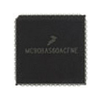
MC68HC11E1CFN3R2 Freescale Semiconductor, MC68HC11E1CFN3R2 Datasheet - Page 156

MC68HC11E1CFN3R2
Manufacturer Part Number
MC68HC11E1CFN3R2
Description
Manufacturer
Freescale Semiconductor
Datasheet
1.MC68HC11E1CFN3R2.pdf
(242 pages)
Specifications of MC68HC11E1CFN3R2
Cpu Family
HC11
Device Core Size
8b
Frequency (max)
3MHz
Interface Type
SCI/SPI
Program Memory Type
ROMLess
Program Memory Size
Not Required
Total Internal Ram Size
512Byte
# I/os (max)
38
Number Of Timers - General Purpose
8
Operating Supply Voltage (typ)
3.3/5V
Operating Supply Voltage (max)
5.5V
Operating Supply Voltage (min)
3V
On-chip Adc
8-chx8-bit
Instruction Set Architecture
CISC
Operating Temp Range
-40C to 85C
Operating Temperature Classification
Industrial
Mounting
Surface Mount
Pin Count
52
Package Type
PLCC
Lead Free Status / Rohs Status
Not Compliant
- Current page: 156 of 242
- Download datasheet (2Mb)
10.9 Control Timing
156
Frequency of operation
E-clock period
Crystal frequency
External oscillator frequency
Processor control setup time
Reset input pulse width
Mode programming setup time
Mode programming hold time
Interrupt pulse width, IRQ edge-sensitive mode
Wait recovery startup time
Timer pulse width input capture pulse accumulator input
Electrical Characteristics
1. V
2. RESET is recognized during the first clock cycle it is held low. Internal circuitry then drives the pin low for four clock cycles,
t
To guarantee external reset vector
Minimum input time (can be pre-empted by internal reset)
PW
PW
PCSU
erwise noted
releases the pin, and samples the pin level two cycles later to determine the source of the interrupt. Refer to
Resets and Interrupts
DD
IRQ
TIM
= 5.0 Vdc ±10%, V
= 1/4 t
= t
= t
CYC
CYC
CYC
+ 20 ns
+ 20 ns
+ 50 ns
Characteristic
for further detail.
SS
= 0 Vdc, T
(1) (2)
A
M68HC11E Family Data Sheet, Rev. 5.1
= T
L
to T
H
, all timing is shown with respect to 20% V
Symbol
PW
PW
PW
t
f
t
t
t
t
PCSU
XTAL
WRS
4 f
MPS
MPH
CYC
f
RSTL
o
IRQ
TIM
o
Min
100
300
102
102
dc
dc
10
—
—
1.0 MHz
0
8
1
2
0
0
Max
1.0
4.0
4.0
—
—
—
—
—
—
—
—
4
Min
500
175
520
520
dc
dc
10
—
—
2.0 MHz
8
1
2
DD
Max
2.0
8.0
8.0
—
—
—
—
—
—
—
—
and 70% V
4
Freescale Semiconductor
Min
333
133
353
353
dc
dc
10
—
—
3.0 MHz
8
1
2
DD
Max
12.0
12.0
3.0
, unless oth-
—
—
—
—
—
—
—
—
4
Chapter 5
MHz
MHz
MHz
Unit
t
t
t
CYC
CYC
CYC
ns
ns
ns
ns
ns
Related parts for MC68HC11E1CFN3R2
Image
Part Number
Description
Manufacturer
Datasheet
Request
R
Part Number:
Description:
Manufacturer:
Freescale Semiconductor, Inc
Datasheet:
Part Number:
Description:
Manufacturer:
Freescale Semiconductor, Inc
Datasheet:
Part Number:
Description:
Manufacturer:
Freescale Semiconductor, Inc
Datasheet:
Part Number:
Description:
Manufacturer:
Freescale Semiconductor, Inc
Datasheet:
Part Number:
Description:
Manufacturer:
Freescale Semiconductor, Inc
Datasheet:
Part Number:
Description:
Manufacturer:
Freescale Semiconductor, Inc
Datasheet:
Part Number:
Description:
Manufacturer:
Freescale Semiconductor, Inc
Datasheet:
Part Number:
Description:
Manufacturer:
Freescale Semiconductor, Inc
Datasheet:
Part Number:
Description:
Manufacturer:
Freescale Semiconductor, Inc
Datasheet:
Part Number:
Description:
Manufacturer:
Freescale Semiconductor, Inc
Datasheet:
Part Number:
Description:
Manufacturer:
Freescale Semiconductor, Inc
Datasheet:
Part Number:
Description:
Manufacturer:
Freescale Semiconductor, Inc
Datasheet:
Part Number:
Description:
Manufacturer:
Freescale Semiconductor, Inc
Datasheet:
Part Number:
Description:
Manufacturer:
Freescale Semiconductor, Inc
Datasheet:
Part Number:
Description:
Manufacturer:
Freescale Semiconductor, Inc
Datasheet:


