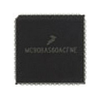
MC68HC11E1CFN3R2 Freescale Semiconductor, MC68HC11E1CFN3R2 Datasheet - Page 163

MC68HC11E1CFN3R2
Manufacturer Part Number
MC68HC11E1CFN3R2
Description
Manufacturer
Freescale Semiconductor
Datasheet
1.MC68HC11E1CFN3R2.pdf
(242 pages)
Specifications of MC68HC11E1CFN3R2
Cpu Family
HC11
Device Core Size
8b
Frequency (max)
3MHz
Interface Type
SCI/SPI
Program Memory Type
ROMLess
Program Memory Size
Not Required
Total Internal Ram Size
512Byte
# I/os (max)
38
Number Of Timers - General Purpose
8
Operating Supply Voltage (typ)
3.3/5V
Operating Supply Voltage (max)
5.5V
Operating Supply Voltage (min)
3V
On-chip Adc
8-chx8-bit
Instruction Set Architecture
CISC
Operating Temp Range
-40C to 85C
Operating Temperature Classification
Industrial
Mounting
Surface Mount
Pin Count
52
Package Type
PLCC
Lead Free Status / Rohs Status
Not Compliant
- Current page: 163 of 242
- Download datasheet (2Mb)
10.12 MC68L11E9/E20 Peripheral Port Timing
Freescale Semiconductor
Frequency of operation
E-clock period
Peripheral data setup time
Peripheral data hold time
Delay time, peripheral data write
Port C input data setup time
Port C input data hold time
Delay time, E fall to STRB
Setup time, STRA asserted to E fall
Delay time, STRA asserted to port C data output valid
Hold time, STRA negated to port C data
3-state hold time
1. V
2. Ports C and D timing is valid for active drive. (CWOM and DWOM bits are not set in PIOC and SPCR registers, respec-
3. If this setup time is met, STRB acknowledges in the next cycle. If it is not met, the response may be delayed one more cycle.
E-clock frequency
MCU read of ports A, C, D, and E
MCU read of ports A, C, D, and E
t
t
PWD
DEB
otherwise noted
tively.)
DD
MCU writes to port A
MCU writes to ports B, C, and D
= 1/4 t
= 1/4 t
= 3.0 Vdc to 5.5 Vdc, V
CYC
CYC
+ 150 ns
+ 150 ns
Characteristic
SS
= 0 Vdc, T
(3)
(1) (2)
Figure 10-7. Port Read Timing Diagram
M68HC11E Family Data Sheet, Rev. 5.1
A
= T
L
to T
H
, all timing is shown with respect to 20% V
Symbol
t
t
t
PDSU
t
t
t
t
t
t
PWD
CYC
PDH
PCD
PCH
DEB
AES
PCZ
t
t
f
IS
IH
o
1000
Min
100
100
dc
50
60
10
—
—
—
—
—
0
1.0 MHz
MC68L11E9/E20 Peripheral Port Timing
Max
250
400
400
100
150
1.0
—
—
—
—
—
—
—
Min
500
100
100
DD
dc
50
60
10
—
—
—
—
—
0
2.0 MHz
and 70% V
Max
250
275
275
100
150
2.0
—
—
—
—
—
—
—
DD
, unless
MHz
Unit
ns
ns
ns
ns
ns
ns
ns
ns
ns
ns
ns
163
Related parts for MC68HC11E1CFN3R2
Image
Part Number
Description
Manufacturer
Datasheet
Request
R
Part Number:
Description:
Manufacturer:
Freescale Semiconductor, Inc
Datasheet:
Part Number:
Description:
Manufacturer:
Freescale Semiconductor, Inc
Datasheet:
Part Number:
Description:
Manufacturer:
Freescale Semiconductor, Inc
Datasheet:
Part Number:
Description:
Manufacturer:
Freescale Semiconductor, Inc
Datasheet:
Part Number:
Description:
Manufacturer:
Freescale Semiconductor, Inc
Datasheet:
Part Number:
Description:
Manufacturer:
Freescale Semiconductor, Inc
Datasheet:
Part Number:
Description:
Manufacturer:
Freescale Semiconductor, Inc
Datasheet:
Part Number:
Description:
Manufacturer:
Freescale Semiconductor, Inc
Datasheet:
Part Number:
Description:
Manufacturer:
Freescale Semiconductor, Inc
Datasheet:
Part Number:
Description:
Manufacturer:
Freescale Semiconductor, Inc
Datasheet:
Part Number:
Description:
Manufacturer:
Freescale Semiconductor, Inc
Datasheet:
Part Number:
Description:
Manufacturer:
Freescale Semiconductor, Inc
Datasheet:
Part Number:
Description:
Manufacturer:
Freescale Semiconductor, Inc
Datasheet:
Part Number:
Description:
Manufacturer:
Freescale Semiconductor, Inc
Datasheet:
Part Number:
Description:
Manufacturer:
Freescale Semiconductor, Inc
Datasheet:


