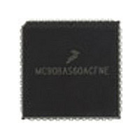
MC68HC11E1CFN3R2 Freescale Semiconductor, MC68HC11E1CFN3R2 Datasheet - Page 42

MC68HC11E1CFN3R2
Manufacturer Part Number
MC68HC11E1CFN3R2
Description
Manufacturer
Freescale Semiconductor
Datasheet
1.MC68HC11E1CFN3R2.pdf
(242 pages)
Specifications of MC68HC11E1CFN3R2
Cpu Family
HC11
Device Core Size
8b
Frequency (max)
3MHz
Interface Type
SCI/SPI
Program Memory Type
ROMLess
Program Memory Size
Not Required
Total Internal Ram Size
512Byte
# I/os (max)
38
Number Of Timers - General Purpose
8
Operating Supply Voltage (typ)
3.3/5V
Operating Supply Voltage (max)
5.5V
Operating Supply Voltage (min)
3V
On-chip Adc
8-chx8-bit
Instruction Set Architecture
CISC
Operating Temp Range
-40C to 85C
Operating Temperature Classification
Industrial
Mounting
Surface Mount
Pin Count
52
Package Type
PLCC
Lead Free Status / Rohs Status
Not Compliant
- Current page: 42 of 242
- Download datasheet (2Mb)
Operating Modes and On-Chip Memory
IRV(NE) — Internal Read Visibility (Not E) Bit
PSEL[3:0] — Priority Select Bits
2.3.3 System Initialization
Registers and bits that control initialization and the basic operation of the MCU are protected against
writes except under special circumstances.
reset or that must be written within the first 64 cycles after reset.
42
SMOD = 0
SMOD = 1
Operating
Mode
IRVNE can be written once in any mode. In expanded modes, IRVNE determines whether IRV is on
or off. In special test mode, IRVNE is reset to 1. In all other modes, IRVNE is reset to 0. For the
MC68HC811E2, this bit is IRV and only controls the internal read visibility function.
In single-chip modes this bit determines whether the E clock drives out from the chip. For the
MC68HC811E2, this bit has no meaning or effect in single-chip and bootstrap modes.
Refer to
0 = No internal read visibility on external bus
1 = Data from internal reads is driven out the external data bus.
0 = E is driven out from the chip.
1 = E pin is driven low. Refer to the following table.
Register
Address
Chapter 5 Resets and
$x03C
$x03D
$x03C
$x03D
$x024
$x035
$x039
$x024
$x035
$x039
Timer interrupt mask 2 (TMSK2)
Block protect register (BPROT)
System configuration options (OPTION)
Highest priority I-bit interrupt
and miscellaneous (HPRIO)
RAM and I/O map register (INIT)
Timer interrupt mask 2 (TMSK2)
Block protect register (BPROT)
System configuration options (OPTION)
Highest priority I-bit interrupt and
miscellaneous (HPRIO)
RAM and I/O map register (INIT)
0
0
Special test
Single chip
Expanded
Bootstrap
Table 2-2. Write Access Limited Registers
Mode
Register Name
Interrupts.
M68HC11E Family Data Sheet, Rev. 5.1
0
1
IRVNE Out
of Reset
Table 2-2
0
0
0
1
Special test
Bootstrap
E Clock Out
lists registers that can be written only once after
of Reset
Bits [1:0], once only
Clear bits, once only
Bits [5:4], bits [2:0], once only
See HPRIO description
Yes, once only
See HPRIO description
On
On
On
On
in First 64 Cycles
Must be Written
1
1
of Reset
IRV Out
—
—
—
—
Off
Off
Off
On
0
1
Affects Only
IRVNE
IRV
IRV
Bits [7:2]
Set bits only
Bits [7:6], bit 3
See HPRIO description
All, set or clear
All, set or clear
All, set or clear
See HPRIO description
All, set or clear
Freescale Semiconductor
E
E
Anytime
Write
—
IRVNE Can
Be Written
Once
Once
Once
Once
Related parts for MC68HC11E1CFN3R2
Image
Part Number
Description
Manufacturer
Datasheet
Request
R
Part Number:
Description:
Manufacturer:
Freescale Semiconductor, Inc
Datasheet:
Part Number:
Description:
Manufacturer:
Freescale Semiconductor, Inc
Datasheet:
Part Number:
Description:
Manufacturer:
Freescale Semiconductor, Inc
Datasheet:
Part Number:
Description:
Manufacturer:
Freescale Semiconductor, Inc
Datasheet:
Part Number:
Description:
Manufacturer:
Freescale Semiconductor, Inc
Datasheet:
Part Number:
Description:
Manufacturer:
Freescale Semiconductor, Inc
Datasheet:
Part Number:
Description:
Manufacturer:
Freescale Semiconductor, Inc
Datasheet:
Part Number:
Description:
Manufacturer:
Freescale Semiconductor, Inc
Datasheet:
Part Number:
Description:
Manufacturer:
Freescale Semiconductor, Inc
Datasheet:
Part Number:
Description:
Manufacturer:
Freescale Semiconductor, Inc
Datasheet:
Part Number:
Description:
Manufacturer:
Freescale Semiconductor, Inc
Datasheet:
Part Number:
Description:
Manufacturer:
Freescale Semiconductor, Inc
Datasheet:
Part Number:
Description:
Manufacturer:
Freescale Semiconductor, Inc
Datasheet:
Part Number:
Description:
Manufacturer:
Freescale Semiconductor, Inc
Datasheet:
Part Number:
Description:
Manufacturer:
Freescale Semiconductor, Inc
Datasheet:


