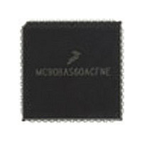
MC68HC11E1CFN3R2 Freescale Semiconductor, MC68HC11E1CFN3R2 Datasheet - Page 53

MC68HC11E1CFN3R2
Manufacturer Part Number
MC68HC11E1CFN3R2
Description
Manufacturer
Freescale Semiconductor
Datasheet
1.MC68HC11E1CFN3R2.pdf
(242 pages)
Specifications of MC68HC11E1CFN3R2
Cpu Family
HC11
Device Core Size
8b
Frequency (max)
3MHz
Interface Type
SCI/SPI
Program Memory Type
ROMLess
Program Memory Size
Not Required
Total Internal Ram Size
512Byte
# I/os (max)
38
Number Of Timers - General Purpose
8
Operating Supply Voltage (typ)
3.3/5V
Operating Supply Voltage (max)
5.5V
Operating Supply Voltage (min)
3V
On-chip Adc
8-chx8-bit
Instruction Set Architecture
CISC
Operating Temp Range
-40C to 85C
Operating Temperature Classification
Industrial
Mounting
Surface Mount
Pin Count
52
Package Type
PLCC
Lead Free Status / Rohs Status
Not Compliant
- Current page: 53 of 242
- Download datasheet (2Mb)
2.5.1.2 EPROM and EEPROM Programming Control Register
The EPROM and EEPROM programming control register (PPROG) selects and controls the EEPROM
programming function. Bits in PPROG enable the programming voltage, control the latching of data to be
programmed, and select the method of erasure (for example, byte, row, etc.).
ODD — Program Odd Rows in Half of EEPROM (Test) Bit
EVEN — Program Even Rows in Half of EEPROM (Test) Bit
ELAT — EPROM/OTPROM Latch Control Bit
BYTE — Byte/Other EEPROM Erase Mode Bit
ROW — Row/All EEPROM Erase Mode Bit
ERASE — Erase Mode Select Bit
EELAT — EEPROM Latch Control Bit
Freescale Semiconductor
For the MC68HC711E9, EPGM enables the high voltage necessary for both EPROM/OTPROM and
EEPROM programming.
For MC68HC711E9, ELAT and EELAT are mutually exclusive and cannot both equal 1.
This bit overrides the ROW bit.
If BYTE is 1, ROW has no meaning.
0 = EPROM address and data bus configured for normal reads
1 = EPROM address and data bus configured for programming
0 = Row or bulk erase
1 = Erase only one byte
0 = Bulk erase
1 = Row erase
0 = Normal read or program mode
1 = Erase mode
0 = EEPROM address and data bus configured for normal reads and cannot be programmed
1 = EEPROM address and data bus configured for programming or erasing and cannot be read
1. MC68HC711E9 only
Address: $103B
Reset:
Read:
Write:
ODD
Bit 7
0
Figure 2-17. EPROM and EEPROM Programming
BYTE
0
0
1
1
EVEN
6
0
M68HC11E Family Data Sheet, Rev. 5.1
Control Register (PPROG)
Table 2-8. EEPROM Erase
ROW
ELAT
0
1
0
1
5
0
(1)
BYTE
Bulk erase (entire array)
Row erase (16 bytes)
Byte erase
Byte erase
4
0
ROW
3
0
Action
ERASE
2
0
EELAT
0
1
EPGM
Bit 0
0
EEPROM
53
Related parts for MC68HC11E1CFN3R2
Image
Part Number
Description
Manufacturer
Datasheet
Request
R
Part Number:
Description:
Manufacturer:
Freescale Semiconductor, Inc
Datasheet:
Part Number:
Description:
Manufacturer:
Freescale Semiconductor, Inc
Datasheet:
Part Number:
Description:
Manufacturer:
Freescale Semiconductor, Inc
Datasheet:
Part Number:
Description:
Manufacturer:
Freescale Semiconductor, Inc
Datasheet:
Part Number:
Description:
Manufacturer:
Freescale Semiconductor, Inc
Datasheet:
Part Number:
Description:
Manufacturer:
Freescale Semiconductor, Inc
Datasheet:
Part Number:
Description:
Manufacturer:
Freescale Semiconductor, Inc
Datasheet:
Part Number:
Description:
Manufacturer:
Freescale Semiconductor, Inc
Datasheet:
Part Number:
Description:
Manufacturer:
Freescale Semiconductor, Inc
Datasheet:
Part Number:
Description:
Manufacturer:
Freescale Semiconductor, Inc
Datasheet:
Part Number:
Description:
Manufacturer:
Freescale Semiconductor, Inc
Datasheet:
Part Number:
Description:
Manufacturer:
Freescale Semiconductor, Inc
Datasheet:
Part Number:
Description:
Manufacturer:
Freescale Semiconductor, Inc
Datasheet:
Part Number:
Description:
Manufacturer:
Freescale Semiconductor, Inc
Datasheet:
Part Number:
Description:
Manufacturer:
Freescale Semiconductor, Inc
Datasheet:


