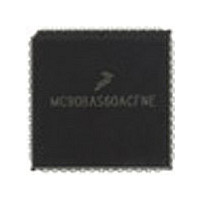
MC68HC11E1CFN3R2 Freescale Semiconductor, MC68HC11E1CFN3R2 Datasheet - Page 80

MC68HC11E1CFN3R2
Manufacturer Part Number
MC68HC11E1CFN3R2
Description
Manufacturer
Freescale Semiconductor
Datasheet
1.MC68HC11E1CFN3R2.pdf
(242 pages)
Specifications of MC68HC11E1CFN3R2
Cpu Family
HC11
Device Core Size
8b
Frequency (max)
3MHz
Interface Type
SCI/SPI
Program Memory Type
ROMLess
Program Memory Size
Not Required
Total Internal Ram Size
512Byte
# I/os (max)
38
Number Of Timers - General Purpose
8
Operating Supply Voltage (typ)
3.3/5V
Operating Supply Voltage (max)
5.5V
Operating Supply Voltage (min)
3V
On-chip Adc
8-chx8-bit
Instruction Set Architecture
CISC
Operating Temp Range
-40C to 85C
Operating Temperature Classification
Industrial
Mounting
Surface Mount
Pin Count
52
Package Type
PLCC
Lead Free Status / Rohs Status
Not Compliant
- Current page: 80 of 242
- Download datasheet (2Mb)
Resets and Interrupts
5.2.2 External Reset (RESET)
The CPU distinguishes between internal and external reset conditions by sensing whether the reset pin
rises to a logic 1 in less than two E-clock cycles after an internal device releases reset. When a reset
condition is sensed, the RESET pin is driven low by an internal device for four E-clock cycles, then
released. Two E-clock cycles later it is sampled. If the pin is still held low, the CPU assumes that an
external reset has occurred. If the pin is high, it indicates that the reset was initiated internally by either
the COP system or the clock monitor.
Do not connect an external resistor capacitor (RC) power-up delay circuit to the reset pin of M68HC11
devices because the circuit charge time constant can cause the device to misinterpret the type of reset
that occurred.
5.2.3 Computer Operating Properly (COP) Reset
The MCU includes a COP system to help protect against software failures. When the COP is enabled, the
software is responsible for keeping a free-running watchdog timer from timing out. When the software is
no longer being executed in the intended sequence, a system reset is initiated.
The state of the NOCOP bit in the CONFIG register determines whether the COP system is enabled or
disabled. To change the enable status of the COP system, change the contents of the CONFIG register
and then perform a system reset. In the special test and bootstrap operating modes, the COP system is
initially inhibited by the disable resets (DISR) control bit in the TEST1 register. The DISR bit can
subsequently be written to 0 to enable COP resets.
The COP timer rate control bits CR[1:0] in the OPTION register determine the COP timeout period. The
system E clock is divided by 2
bits are 0, which selects the fastest timeout period. In normal operating modes, these bits can be written
only once within 64 bus cycles after reset.
80
CR[1:0]
0 0
0 1
1 0
1 1
E/2
Divide
E =
16
64
15
1
4
By
– 0 ms, + 32.8 ms
XTAL = 4.0 MHz
15
131.072 ms
32.768 ms
524.28 ms
Timeout
1.0 MHz
2.098 s
and then further scaled by a factor shown in
Table 5-1. COP Timer Rate Select
M68HC11E Family Data Sheet, Rev. 5.1
– 0 ms, + 16.4 ms
XTAL = 8.0 MHz
CAUTION
16.384 ms
65.536 ms
262.14 ms
Timeout
2.0 MHz
1.049 s
XTAL = 12.0 MHz
– 0 ms, + 10.9 ms
10.923 ms
174.76 ms
43.691 ms
699.05 ms
Timeout
3.0 MHz
Table
XTAL = 16.0 MHz
– 0 ms, + 8.2 ms
Timeout
4.0 MHz
8.19 ms
32.8 ms
5-1. After reset, these
131 ms
524 ms
Freescale Semiconductor
Related parts for MC68HC11E1CFN3R2
Image
Part Number
Description
Manufacturer
Datasheet
Request
R
Part Number:
Description:
Manufacturer:
Freescale Semiconductor, Inc
Datasheet:
Part Number:
Description:
Manufacturer:
Freescale Semiconductor, Inc
Datasheet:
Part Number:
Description:
Manufacturer:
Freescale Semiconductor, Inc
Datasheet:
Part Number:
Description:
Manufacturer:
Freescale Semiconductor, Inc
Datasheet:
Part Number:
Description:
Manufacturer:
Freescale Semiconductor, Inc
Datasheet:
Part Number:
Description:
Manufacturer:
Freescale Semiconductor, Inc
Datasheet:
Part Number:
Description:
Manufacturer:
Freescale Semiconductor, Inc
Datasheet:
Part Number:
Description:
Manufacturer:
Freescale Semiconductor, Inc
Datasheet:
Part Number:
Description:
Manufacturer:
Freescale Semiconductor, Inc
Datasheet:
Part Number:
Description:
Manufacturer:
Freescale Semiconductor, Inc
Datasheet:
Part Number:
Description:
Manufacturer:
Freescale Semiconductor, Inc
Datasheet:
Part Number:
Description:
Manufacturer:
Freescale Semiconductor, Inc
Datasheet:
Part Number:
Description:
Manufacturer:
Freescale Semiconductor, Inc
Datasheet:
Part Number:
Description:
Manufacturer:
Freescale Semiconductor, Inc
Datasheet:
Part Number:
Description:
Manufacturer:
Freescale Semiconductor, Inc
Datasheet:


