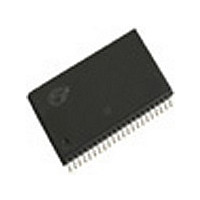
CY7C1041BV33L-15ZC Cypress Semiconductor Corp, CY7C1041BV33L-15ZC Datasheet

CY7C1041BV33L-15ZC
Specifications of CY7C1041BV33L-15ZC
Related parts for CY7C1041BV33L-15ZC
CY7C1041BV33L-15ZC Summary of contents
Page 1
... DECODER Selection Guide Maximum Access Time (ns) Maximum Operating Current (mA) Comm’l Maximum CMOS Standby Current (mA) Cypress Semiconductor Corporation Document #: 38-05168 Rev. ** written into the location specified on the address pins (A through A from I/O pins (I/O specified on the address pins (A Reading from the device is accomplished by taking Chip Enable (CE) and Output Enable (OE) LOW while forcing the Write Enable (WE) HIGH ...
Page 2
Maximum Ratings (Above which the useful life may be impaired. For user guide- lines, not tested.) Storage Temperature ................................. – +150 C Ambient Temperature with Power Applied............................................. – +125 C [1] Supply Voltage ...
Page 3
Electrical Characteristics Over the Operating Range (continued) Parameter Description V Output HIGH Voltage OH V Output LOW Voltage OL V Input HIGH Voltage IH [1] V Input LOW Voltage IL I Input Load Current IX I Output Leakage OZ Current ...
Page 4
Switching Characteristics Over the Operating Range Parameter Description READ CYCLE t Read Cycle Time RC t Address to Data Valid AA t Data Hold from Address Change OHA t CE LOW to Data Valid ACE t OE LOW to ...
Page 5
Switching Characteristics Over the Operating Range (continued) Parameter Description READ CYCLE t Read Cycle Time RC t Address to Data Valid AA t Data Hold from Address Change OHA t CE LOW to Data Valid ACE t OE LOW ...
Page 6
Data Retention Waveform Switching Waveforms [11, 12] Read Cycle No. 1 ADDRESS DATA OUT PREVIOUS DATA VALID [12, 13] Read Cycle No. 2 (OE Controlled) ADDRESS CE t ACE OE t DOE BHE, BLE t LZOE t ...
Page 7
Switching Waveforms (continued) [14, 15] Write Cycle No. 1 (CE Controlled) ADDRESS BHE, BLE DATAI/O Write Cycle No. 2 (BLE or BHE Controlled) ADDRESS t SA BHE, BLE WE CE DATAI/O Notes: 14. Data I/O is ...
Page 8
Switching Waveforms (continued) Write Cycle No.3 (WE Controlled, OE LOW) ADDRESS BHE, BLE DATA I/O Truth Table BLE BHE High Data Out ...
Page 9
... Ordering Information Speed (ns) Ordering Code 12 CY7C1041BV33-12VC CY7C1041BV33L-12VC CY7C1041BV33-12ZC CY7C1041BV33L-12ZC 15 CY7C1041BV33-15VC CY7C1041BV33L-15VC CY7C1041BV33-15ZC CY7C1041BV33L-15ZC CY7C1041BV33-15VI CY7C1041BV33-15ZI 17 CY7C1041BV33-17VC CY7C1041BV33L-17VC CY7C1041BV33-17ZC CY7C1041BV33L-17ZC CY7C1041BV33-17VI CY7C1041BV33-17ZI 20 CY7C1041BV33-20VC CY7C1041BV33L-20VC CY7C1041BV33-20ZC CY7C1041BV33L-20ZC CY7C1041BV33-20VI CY7C1041BV33-20ZI 25 CY7C1041BV33-25VC CY7C1041BV33L-25VC CY7C1041BV33-25ZC CY7C1041BV33L-25ZC CY7C1041BV33-25VI CY7C1041BV33-25ZI Document #: 38-05168 Rev. ** Package Name Package Type V34 ...
Page 10
... Document #: 38-05168 Rev. ** © Cypress Semiconductor Corporation, 2001. The information contained herein is subject to change without notice. Cypress Semiconductor Corporation assumes no responsibility for the use of any circuitry other than circuitry embodied in a Cypress Semiconductor product. Nor does it convey or imply any license under patent or other rights. Cypress Semiconductor does not authorize its products for use as critical components in life-support systems where a malfunction or failure may reasonably be expected to result in significant injury to the user ...
Page 11
... Document Title: CY7C1041BV33 256K x 16 SRAM Document Number: 38-05168 Issue REV. ECN NO. Date Change ** 111840 11/17/01 Document #: 38-05168 Rev. ** Orig. of Description of Change DSG Change from Spec number: 38-00932 to 38-05168 CY7C1041BV33 Page [+] Feedback ...


