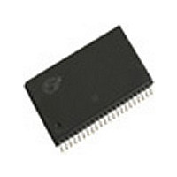
CY7C1049CV33-12ZI Cypress Semiconductor Corp, CY7C1049CV33-12ZI Datasheet

CY7C1049CV33-12ZI
Specifications of CY7C1049CV33-12ZI
Related parts for CY7C1049CV33-12ZI
CY7C1049CV33-12ZI Summary of contents
Page 1
... Document #: 38-05006 Rev. *H 4-Mbit (512K X 8) Static RAM Functional Description The CY7C1049CV33 is a high performance CMOS Static RAM organized as 524,288 words by eight bits. Easy memory expansion is provided by an active LOW Chip Enable (CE), an active LOW Output Enable (OE), and three-state drivers. Writing to the device is accomplished by taking Chip Enable (CE) and Write Enable (WE) inputs LOW ...
Page 2
... Pin Configuration ............................................................. 3 Selection Guide ................................................................ 3 Pin Definitions .................................................................. 4 Maximum Ratings............................................................. 5 Operating Range............................................................... 5 Electrical Characteristics................................................. 5 Capacitance ...................................................................... 5 Thermal Resistance.......................................................... 5 Document #: 38-05006 Rev. *H CY7C1049CV33 AC Switching Characteristics ......................................... 7 Switching Waveforms ...................................................... 8 Truth Table........................................................................ 9 Ordering Information ....................................................... 9 Package Diagrams ......................................................... 10 Document History Page................................................. 11 Sales, Solutions, and Legal Information ...................... 12 Worldwide Sales and Design Support....................... 12 Products ...
Page 3
... I Selection Guide Maximum Access Time Maximum Operating Current Maximum CMOS Standby Current Document #: 38-05006 Rev. *H Figure 2. 44-Pin TSOP II (Top View I/O 7 I/O 6 GND V CC I Description Commercial Industrial/Automotive-A Automotive-E Commercial/Industrial/ Automotive-A Automotive-E CY7C1049CV33 I I I/O I I/O ...
Page 4
... When LOW, the I/O pins are allowed to behave as outputs. When deasserted HIGH, I/O pins are three-stated, and act as input data pins. Ground Ground for the device. Should be connected to ground of the system. Power Supply Power supply inputs to the device. CY7C1049CV33 Description Page [+] Feedback ...
Page 5
... Test Conditions T = 25 MHz 3.3V CC Test Conditions Test conditions follow standard test methods and procedures for measuring thermal impedance, per EIA / JESD51. CY7C1049CV33 [2] ...................................... –0. Ambient Temperature V CC 3.3V 0.3V 0C to +70C –40C to +85C –40C to +125C -10 ...
Page 6
... Figure (b). High-Z characteristics are tested for all speeds using the test load shown in Figure (d). Document #: 38-05006 Rev. *H Figure 3. AC Test Loads and Waveforms 50 30 pF* 1.5V (a) High-Z characteristics: ALL INPUT PULSES 90% 10% (c) Fall Time: 1 V/ns CY7C1049CV33 [3] 12-, 15-ns devices: R 317 3.3V OUTPUT 351 (b) R 317 3.3V OUTPUT ...
Page 7
... Min Max Min 100 100 values until the first memory access can be performed less than less than t , and t HZCE LZCE HZOE LZOE HZWE and t HZWE CY7C1049CV33 -12 -15 Max Min Max 100 less than t for any given device. LZWE . SD Page Unit ...
Page 8
... If CE goes HIGH simultaneously with WE HIGH, the output remains in high impedance state. 16. During this period, the I/Os are in output state. Do not apply input signals. Document #: 38-05006 Rev OHA DOE DATA VALID 50 SCE PWE t SD DATA VALID CY7C1049CV33 [11, 12] DATA VALID [12, 13] t HZOE t HZCE HIGH IMPEDANCE 50 [14, 15 Page [+] Feedback ...
Page 9
... High Data Out Data High-Z Ordering Information Speed (ns) Ordering Code 10 CY7C1049CV33-10VXC CY7C1049CV33-10VXA 12 CY7C1049CV33-12ZSXA 15 CY7C1049CV33-15VXE CY7C1049CV33-15ZSXE Document #: 38-05006 Rev SCE PWE t SD DATA VALID –I/O Mode 7 Power Down Read Write Selected, Outputs Disabled Package Diagram Package Type 51-85090 36-Pin (400-Mil) Molded SOJ (Pb-Free) ...
Page 10
... Figure 8. 36-Pin (400-Mil) Molded SOJ V36, 51-85090 .920 .930 .026 .050 .032 TYP. .015 .020 Document #: 38-05006 Rev. *H PIN 1 I.D .435 .445 .395 .405 .128 .148 SEATING PLANE .025 MIN. Figure 9. 44-Pin TSOP II, 51-85087 CY7C1049CV33 .007 .013 .360 .380 DIMENSIONS IN INCHES MIN. MAX. 51-85090 *D 51-85087 *C Page [+] Feedback ...
Page 11
... Document History Page Document Title: CY7C1049CV33 4-Mbit (512K X 8) Static RAM Document Number: 38-05006 Rev. ECN Orig. of Submission Change Date ** 112569 HGK 03/06/02 *A 114091 DFP 04/25/02 *B 116479 CEA 09/16/02 *C 262949 RKF See ECN *D 300091 RKF See ECN *E 344595 SYT See ECN ...
Page 12
... Cypress against all charges. Use may be limited by and subject to the applicable Cypress software license agreement. Document #: 38-05006 Rev. *H All products and company names mentioned in this document may be the trademarks of their respective holders. cypress.com/go/plc Revised March 25, 2010 CY7C1049CV33 PSoC Solutions psoc.cypress.com/solutions PSoC 1 | PSoC 3 ...


