CY7C68013-128AC Cypress Semiconductor Corp, CY7C68013-128AC Datasheet
CY7C68013-128AC
Specifications of CY7C68013-128AC
Available stocks


Related parts for CY7C68013-128AC


CY7C68013-128AC Summary of contents
Page 1
... CY 8.5 kB Smart RAM USB 1.1/2.0 Engine “Soft Configuration” Easy firmware changes Figure 1-1. Block Diagram • 3901 North First Street CY7C68013 2 C-compatible controller, runs at 100 or 400 Compatible Master Abundant I/O Additional I/Os (24) including two USARTS General ADDR (9) programmable I/F ...
Page 2
... The four I/O ports A–D use the SFR addresses used in the standard 8051 for ports 0–3, which are not imple- mented in FX2. Because of the faster and more efficient SFR addressing, the FX2 I/O ports are not addressable in external RAM space (using the MOVX instruction). CY7C68013 Page ...
Page 3
... To do this, the FX2 must enumerate in the full speed mode and then, when configured, renumerate in high speed mode. For an example of the benefits and limitations of this renumeration process see the application note titled “Bus Powered Enumeration with FX2”. CY7C68013 SCON1 ...
Page 4
... EP8 OUT was Pinged and it NAK’d Bus errors exceeded the programmed limit reserved reserved reserved ISO EP2 OUT PID sequence error ISO EP4 OUT PID sequence error ISO EP6 OUT PID sequence error ISO EP8 OUT PID sequence error CY7C68013 Notes Page ...
Page 5
... USB download • USB upload • Setup data pointer 2 • I C-compatible interface boot load. 3.10.3 External Code Memory The bottom eight kbytes of program memory is external, and therefore the bottom eight kbytes of internal RAM is accessible only as data memory. CY7C68013 Notes Page ...
Page 6
... Eight kbytes data memory RAM here—RD#/WR# Data strobes are not (RD#,WR#)* active) Data 2 C-compatible interface boot access Figure 3-2. External Code Memory CY7C68013 56 kbytes External Code Memory (PSEN#) (OK to populate program memory here— PSEN# strobe is not active) Code 64 kbytes ...
Page 7
... EP6&8, since none of the 512-byte buffers are combined between these endpoint groups. An example endpoint config- uration would be: EP2—1024 double buffered; EP6—512 quad buffered. To the right of the vertical line, buffers are shared between EP2–8, and therefore only entire columns may be chosen. CY7C68013 Page ...
Page 8
... CY7C68013 1024 1024 1024 1024 EP2 ...
Page 9
... GPIF The GPIF is a flexible 8- or 16-bit parallel interface driven by a user-programmable finite state machine. It allows the CY7C68013 to perform local bus mastering, and can implement a wide variety of protocols such as ATA interface, printer parallel port, and Utopia. The GPIF has six programmable control outputs (CTL), nine address outputs (GPIFADRx), and six general-purpose ready inputs (RDY) ...
Page 10
... Note that two of the required signals, RD# and WR#, are present in the 100-pin version. In the 100-pin and 128-pin versions, an 8051 control bit can be set to pulse the RD# and WR# pins when the 8051 reads from/writes to PORTC. CY7C68013 2 I C-compatible Interface Boot Load Access 2 ...
Page 11
... D5 PSEN A15 D2 A14 D1 A13 D0 A12 A11 A10 128 Figure 4-1. Signals CY7C68013 Slave FIFO FD[15] FD[14] FD[13] FD[12] FD[11] FD[10] FD[9] FD[8] FD[7] FD[6] FD[5] FD[4] FD[3] FD[2] FD[1] FD[0] SLRD SLWR FLAGA FLAGB FLAGC INT0#/ PA0 INT1#/ PA1 SLOE WU2/PA3 ...
Page 12
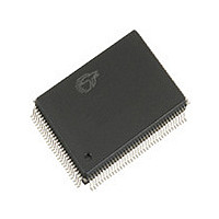
... A14 25 A15 VCC 26 GND 27 28 INT4 IFCLK 32 33 RESERVED 34 BKPT SCL 37 SDA OE# 38 Figure 4-2. CY7C68013 128-pin TQFP Pin Assignment Document #: 38-08012 Rev. *F CY7C68013 128-pin TQFP * denotes programmable polarity CY7C68013 102 PD0/FD8 101 *WAKEUP 100 VCC 99 RESET# 98 CTL5 GND 92 PA7/*FLAGD/SLCS# 91 ...
Page 13
... DMINUS 18 GND 19 VCC 20 GND 21 INT4 IFCLK 26 RESERVED 27 BKPT 28 SCL 29 SDA 30 Figure 4-3. CY7C68013 100-pin TQFP Pin Assignment Document #: 38-08012 Rev. *F PA7/*FLAGD/SLCS# CY7C68013 100-pin TQFP * denotes programmable polarity CY7C68013 PD0/FD8 80 *WAKEUP 79 VCC 78 RESET# 77 CTL5 76 GND 75 74 PA6/*PKTEND 73 PA5/FIFOADR1 72 PA4/FIFOADR0 71 PA3/*WU2 ...
Page 14
... Figure 4-4. CY7C68013 56-pin SSOP Pin Assignment Document #: 38-08012 Rev. *F CY7C68013 56-pin SSOP PD5/FD13 PD4/FD12 1 PD6/FD14 PD3/FD11 2 PD7/FD15 PD2/FD10 3 GND PD1/FD9 4 CLKOUT PD0/FD8 5 VCC *WAKEUP 6 GND 7 RDY0/*SLRD RESET# 8 RDY1/*SLWR 9 AVCC PA7/*FLAGD/SLCS# 10 XTALOUT PA6/PKTEND 11 XTALIN PA5/FIFOADR1 12 AGND PA4/FIFOADR0 13 VCC ...
Page 15
... XTALOUT 4 XTALIN 5 AGND 6 VCC 7 DPLUS 8 DMINUS 9 GND 10 VCC 11 GND 12 *IFCLK 13 RESERVED 14 Figure 4-5. CY7C68013 56-pin QFN Pin Assignment Document #: 38-08012 Rev. *F CY7C68013 56-pin QFN * denotes programmable polarity CY7C68013 RESET# 42 GND 41 PA7/*FLAGD/SLCS# 40 PA6/*PKTEND 39 PA5/FIFOADR1 38 PA4/FIFOADR0 37 PA3/*WU2 36 PA2/*SLOE 35 PA1/INT1# ...
Page 16
... CY7C68013 Pin Descriptions [5] Table 4-1. FX2 Pin Descriptions 128 100 56 56 TQFP TQFP SSOP QFN Name AVCC AGND DMINUS DPLUS 117 A4 118 A5 119 A6 120 A7 126 A8 127 A9 128 A10 21 A11 22 A12 23 A13 24 A14 25 A15 PSEN BKPT RESET# Note: 5. Unused inputs should not be left floating. Tie either HIGH or LOW as appropriate. Outputs should only be pulled up or down to ensure signals at power-up and in standby ...
Page 17
... FIFOADR1 is an input-only address select for the slave FIFOs connected to FD[7..0] or FD[15..0]. I/O/Z I Multiplexed pin whose function is selected by the IFCONFIG[1:0] (PA6) bits. PA6 is a bidirectional I/O port pin. PKTEND is an input-only packet end with programmable polarity (FIFOPOLAR.5) for the slave FIFOs connected to FD[7..0] or FD[15..0]. CY7C68013 Description Page ...
Page 18
... Multiplexed pin whose function is selected by PORTCCFG.3 (PC3) PC3 is a bidirectional I/O port pin. GPIFADR3 is a GPIF address output pin. I/O/Z I Multiplexed pin whose function is selected by PORTCCFG.4 (PC4) PC4 is a bidirectional I/O port pin. GPIFADR4 is a GPIF address output pin. CY7C68013 Description Page ...
Page 19
... PE1 is a bidirectional I/O port pin. T1OUT is an active-HIGH signal from 8051 Timer-counter1. T1OUT outputs a high level for one CLKOUT clock cycle when Timer1 overflows. If Timer1 is operated in Mode 3 (two separate timer/counters), T1OUT is active when the low byte timer/counter overflows. CY7C68013 Description Page ...
Page 20
... SLWR is the input-only write strobe with programmable polarity (FIFOPOLAR.2) for the slave FIFOs connected to FDI[7..0] or FDI[15..0]. Input N/A RDY2 is a GPIF input signal. Input N/A RDY3 is a GPIF input signal. Input N/A RDY4 is a GPIF input signal. Input N/A RDY5 is a GPIF input signal. CY7C68013 Description Page ...
Page 21
... TXD0 is the active-HIGH TXD0 output from 8051 UART0, which provides the output clock in sync mode, and the output data in async mode. Output H CS# is the active-LOW chip select for external memory. Output H WR# is the active-LOW write strobe output for external memory. CY7C68013 Description Page ...
Page 22
... Ground N/A Ground. N/A N/A No-connect. This pin must be left open. N/A N/A No-connect. This pin must be left open. N/A N/A No-connect. This pin must be left open. CY7C68013 Description CC 2 C-compatible peripheral is attached. with a 2. C-compatible peripheral is attached. Page with a ...
Page 23
... PL7 PL6 PL5 PL4 PL7 PL6 PL5 PL4 DECIS PKTSTAT IN:PKTS[2] IN:PKTS[1] OUT:PFC12 OUT:PFC11 DECIS PKTSTAT OUT:PFC12 OUT:PFC11 OUT:PFC10 PFC7 PFC6 PFC5 PFC4 CY7C68013 CLKSPD0 CLKINV CLKOE 8051RES ASYNC GSTATE IFCFG1 IFCFG0 FLAGA3 FLAGA2 FLAGA1 FLAGA0 FLAGC3 FLAGC2 FLAGC1 FLAGC0 EP3 ...
Page 24
... ISOEP8 ISOEP6 ISOEP4 ISOEP2 ISOEP8 ISOEP6 ISOEP4 ISOEP2 EC3 EC2 EC1 EC0 I2V4 I2V3 I2V2 1 0 I4V3 I4V2 CY7C68013 PFC3 PFC2 PFC1 PFC0 IN: PKTS[ PFC8 OUT:PFC9 0 0 PFC8 PFC3 PFC2 PFC1 PFC0 PFC3 PFC2 PFC1 PFC0 IN:PKTS[0] 0 PFC9 PFC8 OUT:PFC10 ...
Page 25
... NPAK2 NPAK1 NPAK0 0 0 NPAK1 NPAK0 0 NPAK2 NPAK1 NPAK0 0 0 NPAK1 NPAK0 BC12 CY7C68013 INT1 INT0 GPIFA3 GPIFA2 GPIFA1 GPIFA0 RXD0OUT T2OUT T1OUT T0OUT ID0 BERR ACK DONE STOPIE 400KHZ CRC11 CRC10 CRC9 CRC8 CRC3 CRC2 CRC1 CRC0 QSTATE QSIGNAL2 QSIGNAL1 ...
Page 26
... TC22 TC21 TC20 TC15 TC14 TC13 TC12 TC7 TC6 TC5 TC4 CY7C68013 BC3 BC2 BC1 BC0 00000000 0 BC10 BC9 BC8 00000000 BC3 BC2 BC1 BC0 00000000 BC11 BC10 BC9 BC8 00000000 BC3 BC2 BC1 BC0 00000000 0 BC10 BC9 BC8 00000000 BC3 ...
Page 27
... D5 D4 D15 D14 D13 D12 D15 D14 D13 D12 x x T2M T1M IE5 IE4 I²CINT USBNT A15 A14 A13 A12 SM0_0 SM1_0 SM2_0 REN_0 CY7C68013 Default 0 0 FS1 FS0 00000000 FIFO6FLAG 00000000 xxxxxxxx 0 0 FS1 FS0 00000000 FIFO8FLAG 00000000 xxxxxxxx D11 ...
Page 28
... SM2_1 REN_1 TF2 EXF2 RCLK TCLK D15 D14 D13 D12 RS1 SMOD1 1 ERESI RESI EX6 PX6 CY7C68013 Default A11 A10 A9 A8 00000000 00000000 A11 A10 A9 A8 00000000 00000000 xxxxxxxx xxxxxxxx xxxxxxxx ET1 EX1 ET0 EX0 00000000 EP4F EP4E EP2F EP2E 01011010 ...
Page 29
... Document #: 38-08012 Rev. *F Conditions 0< V < OUT I = –4 mA OUT Except D+/D– D+/D– Connected Disconnected 8051 running, connected to USB HS 8051 running, connected to USB FS V min. = 3.0V CC CY7C68013 Parallel Resonant Min. Typ. Max. Unit 3.0 3.3 3 5.25 V –0.5 0.8 V µA ±10 2.4 V 0.4 ...
Page 30
... ACC1 t (24 MHz) = 3*t – t –t = 106 ns ACC1 CL AV DSU t (48 MHz) = 3*t – t – ns. ACC1 CL AV DSU Document #: 38-08012 Rev STBH STBL [11 ACC1 data in Min 9.6 0 CY7C68013 t AV Typ. Max. Unit 20.83 ns 41.66 ns 83 Page Notes 48 MHz 24 MHz 12 MHz ...
Page 31
... ACC3 CL AV DSU Document #: 38-08012 Rev. *F Stretch = STBL STBH t SCSL t SOEL t DSU [12 ACC1 data in Stretch = 1 [12] t ACC1 Figure 9-2. Data Memory Read Timing Diagram Min. 9.6 0 CY7C68013 DSU t DH data in Typ. Max. Unit 20.83 ns 41.66 ns 83 Page Notes 48 MHz ...
Page 32
... RD# or WR# are active. The address of AUTOPTR2 will be active throughout the cycle and meet the above address valid time for which is based on the stretch value. Document #: 38-08012 Rev STBL STBH data out Stretch = 1 data out Figure 9-3. Data Memory Write Timing Diagram Description CY7C68013 OFF1 Min. Max. Unit 0 10 ...
Page 33
... IFCLK must not exceed 48 MHz. Document #: 38-08012 Rev IFCLK t SGA X t SRY t RYH valid t t SGD DAH X t XCTL N N+1 t XGD Description Output Propagation Delay Description Output Propagation Delay CY7C68013 [13] [14, 15] Min. Max. Unit 20. 6.7 ns [15] Min. Max. Unit 20.83 ...
Page 34
... SLOE Turn-off to FIFO Data Hold OEoff t Clock to FLAGS Output Propagation Delay XFLG t Clock to FIFO Data Output Propagation Delay XFD Document #: 38-08012 Rev IFCLK t RDH t SRD t XFLG N OEon XFD Description Description CY7C68013 t OEoff [13] [15] Min. Max. Unit 20. 10.5 ns 10 [15] Min. Max. ...
Page 35
... Slave FIFO asynchronous parameter values use internal IFCLK setting at 48 MHz. Document #: 38-08012 Rev RDpwl t XFD N N+1 t OEon [16] Description t IFCLK t WRH t SWR SFD FDH t XFLG Description CY7C68013 t RDpwh t XFLG t OEoff [13] Min. Max 10.5 10.5 Z [13] [15] Min. Max. 20.83 18.1 0 9.2 0 9.5 ...
Page 36
... Clock to PKTEND Hold Time PEH t Clock to FLAGS Output Propagation Delay XFLG Document #: 38-08012 Rev. *F Description t WRpwh t WRpwl t t FDH SFD t XFD Description t PEH t SPE t XFLG Description CY7C68013 [15] Min. Max. Unit 20.83 200 ns 12.1 ns 3.6 ns 3.2 ns 4.5 ns 13.5 ns [13] [16] Min. Max. Unit 50 ns ...
Page 37
... Failing to adhere to this timing, will result in the FX2 failing to send the one byte/word short packet FDH SFD FDH FDH SFD SFD X-2 X-1 X-3 CY7C68013 [15] Min. Max. 20.83 200 8.6 2.5 13.5 t FAH >= t WRH ...
Page 38
... FIFOADR[1:0] to FLAGS Output Propagation Delay XFLG t FIFOADR[1:0] to FIFODATA Output Propagation Delay XFD Document #: 38-08012 Rev PEpwh t PEpwl t XFLG [16] Description t OEoff t OEon Description t XFLG t XFD N N+1 Description CY7C68013 [13] Min. Max. Unit 115 ns [13] Min. Max. Unit 10.5 ns 10.5 ns [13] Min. Max. Unit 10.7 ns 14.3 ...
Page 39
... Table 9-17. Slave FIFO Asynchronous Address Parameters Parameter t FIFOADR[1:0] to RD/WR/PKTEND Set-up Time SFA t SLRD/PKTEND to FIFOADR[1:0] Hold Time FAH t SLWR/PKTEND to FIFOADR[1:0] Hold Time FAH Document #: 38-08012 Rev SFA FAH [15] Description t SFA [16] Description CY7C68013 Min. Max. Unit 20.83 200 FAH [13] Min. Max. Unit ...
Page 40
... During the first read cycle, on the rising edge of the clock the FIFO pointer is updated and increments to point to address N+1. For each subsequent rising edge of IFCLK, while the SLRD is asserted, the FIFO pointer is incre- mented and the next data value is placed on the data bus. CY7C68013 >= t RDH t t ...
Page 41
... PKTEND pin at least one clock cycle after the rising edge that caused the last byte/word to be clocked into the previous auto committed packet (the packet with the number of bytes equal to what is set in the AUTOINLEN register). Refer to Figure 9- 10 for further details on this timing. CY7C68013 t FAH >= t WRH ...
Page 42
... through 5. Note: In burst read mode, during SLOE is assertion, the data bus driven state and outputs the previous data. Once SLRD is asserted, the data from the FIFO is driven on the data bus (SLOE must also be asserted) and then the FIFO pointer is incremented. CY7C68013 t FAH t t ...
Page 43
... It should be designed to assert the PKTEND after SLWR is deasserted and met the minimum de- before the SFD asserted pulse width. The FIFOADDR lines are to be held constant during the PKTEND assertion. from the XFLG CY7C68013 t FAH t t WRpwl WRpwh T=9 ...
Page 44
... Ordering Information Table 10-1. Ordering Information Ordering Code CY7C68013-128AC 128 TQFP CY7C68013-100AC 100 TQFP CY7C68013-56PVC 56 SSOP CY7C68013-56LFC 56 QFN CY7C68013-128AXC 128 TQFP Lead-Free Package CY7C68013-100AXC 100 TQFP Lead-Free Package CY7C68013-56PVXC 56 SSOP Lead-Free Package CY7C68013-56LFXC 56 QFN Lead-Free Package CY3681 EZ-USB FX2 Xcelerator Development Kit Document #: 38-08012 Rev ...
Page 45
... Document #: 38-08012 Rev. *F SIDE VIEW 0.08[0.003] C 1.00[0.039] MAX. 0.05[0.002] MAX. 0.80[0.031] MAX. 0.20[0.008] REF. 0.30[0.012] 0.50[0.020] 0°-12° C SEATING PLANE Figure 11-2. 56-Lead QFN LF56A CY7C68013 51-85062-*C BOTTOM VIEW 0.18[0.007] 0.28[0.011] PIN1 ID N 0.20[0.008 0.45[0.018] E-PAD (PAD SIZE VARY BY DEVICE TYPE) 0.24[0.009] (4X) 0 ...
Page 46
... Figure 11-3. 100-Pin Thin Plastic Quad Flatpack ( 1.4 mm) A101 Figure 11-4. 128-Lead Thin Plastic Quad Flatpack ( 1.4 mm) A128 Document #: 38-08012 Rev. *F CY7C68013 51-85050-*A 51-85101-*B Page ...
Page 47
... PCB Material This figure only shows the top three layers of the circuit board: Top Solder, PCB Dielectric, and the Ground Plane Figure 13-3. X-ray Image of the Assembly 2 C system, provided that the system conforms to the I CY7C68013 2 C Standard Specification Page ...
Page 48
... Document History Page Document Title: CY7C68013 EZ-USB FX2™ USB Microcontroller High-speed USB Peripheral Controller Document Number: 38-08012 REV. ECN NO. Issue Date ** 111753 11/15/01 *A 111802 02/20/02 *B 115480 06/26/02 *C 120776 01/06/03 *D 288810 See ECN *E 317674 See ECN *F 352234 See ECN Document #: 38-08012 Rev. *F Orig ...