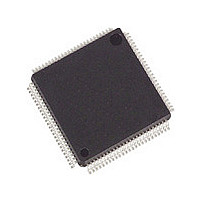
M30626FHPGP Renesas Electronics America, M30626FHPGP Datasheet - Page 32

M30626FHPGP
Manufacturer Part Number
M30626FHPGP
Description
Manufacturer
Renesas Electronics America
Datasheet
1.M30626FHPGP.pdf
(103 pages)
Specifications of M30626FHPGP
Cpu Family
M16C
Device Core Size
16/32Bit
Frequency (max)
24MHz
Interface Type
I2C/IEBus/UART
Program Memory Type
Flash
Program Memory Size
384KB
Total Internal Ram Size
31KB
# I/os (max)
87
Number Of Timers - General Purpose
11
Operating Supply Voltage (typ)
5V
Operating Supply Voltage (max)
5.5V
Operating Supply Voltage (min)
3.3V
On-chip Adc
26-chx10-bit
On-chip Dac
2-chx8-bit
Instruction Set Architecture
CISC
Operating Temp Range
-20C to 85C
Operating Temperature Classification
Commercial
Mounting
Surface Mount
Pin Count
100
Package Type
LQFP
Lead Free Status / Rohs Status
Compliant
Available stocks
Company
Part Number
Manufacturer
Quantity
Price
Company:
Part Number:
M30626FHPGP
Manufacturer:
RENESAS
Quantity:
24
Part Number:
M30626FHPGP
Manufacturer:
RENESAS/瑞萨
Quantity:
20 000
Company:
Part Number:
M30626FHPGP#U3C
Manufacturer:
Renesas
Quantity:
300
Company:
Part Number:
M30626FHPGP#U3C
Manufacturer:
Renesas
Quantity:
834
Company:
Part Number:
M30626FHPGP#U3C
Manufacturer:
Renesas Electronics America
Quantity:
10 000
Part Number:
M30626FHPGP#U5
Manufacturer:
RENESAS/瑞萨
Quantity:
20 000
Company:
Part Number:
M30626FHPGP#U5C
Manufacturer:
Renesas Electronics America
Quantity:
10 000
Part Number:
M30626FHPGP#U5C
Manufacturer:
RENESAS/瑞萨
Quantity:
20 000
Company:
Part Number:
M30626FHPGP#U7C
Manufacturer:
Renesas Electronics America
Quantity:
10 000
M16C/62P Group (M16C/62P, M16C/62PT)
Rev.2.41
REJ03B0001-0241
2.
Figure 2.1 shows the CPU registers. The CPU has 13 registers. Of these, R0, R1, R2, R3, A0, A1 and FB comprise a
register bank. There are two register banks.
Figure 2.1
2.1
The R0 register consists of 16 bits, and is used mainly for transfers and arithmetic/logic operations. R1 to R3 are
the same as R0.
The R0 register can be separated between high (R0H) and low (R0L) for use as two 8-bit data registers.
R1H and R1L are the same as R0H and R0L. Conversely, R2 and R0 can be combined for use as a 32-bit data
register (R2R0). R3R1 is the same as R2R0.
Central Processing Unit (CPU)
Data Registers (R0, R1, R2 and R3)
b31
Jan 10, 2006
Central Processing Unit Register
NOTES:
1. These registers comprise a register bank. There are two register banks.
R2
R3
Page 30 of 96
b15
IPL
b19
b19
INTBH
b15
b15
b15
b15
R0H
R1H
b8
b7
U
PC
I
INTBL
b8 b7
USP
FLG
ISP
SB
R2
R3
A0
A1
FB
O
B
S
R0L
R1L
Z
D
C
b0
b0
b0
b0
b0
b0
2. Central Processing Unit (CPU)
Data Registers
Address Registers
Frame Base Registers
Interrupt Table Register
Program Counter
User Stack Pointer
Interrupt Stack Pointer
Static Base Register
Flag Register
Carry Flag
Debug Flag
Zero Flag
Sign Flag
Register Bank Select Flag
Overflow Flag
Interrupt Enable Flag
Stack Pointer Select Flag
Reserved Area
Processor Interrupt Priority Level
Reserved Area
(1)
(1)
(1)


