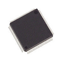
M30626FHPGP Renesas Electronics America, M30626FHPGP Datasheet - Page 57

M30626FHPGP
Manufacturer Part Number
M30626FHPGP
Description
Manufacturer
Renesas Electronics America
Datasheet
1.M30626FHPGP.pdf
(103 pages)
Specifications of M30626FHPGP
Cpu Family
M16C
Device Core Size
16/32Bit
Frequency (max)
24MHz
Interface Type
I2C/IEBus/UART
Program Memory Type
Flash
Program Memory Size
384KB
Total Internal Ram Size
31KB
# I/os (max)
87
Number Of Timers - General Purpose
11
Operating Supply Voltage (typ)
5V
Operating Supply Voltage (max)
5.5V
Operating Supply Voltage (min)
3.3V
On-chip Adc
26-chx10-bit
On-chip Dac
2-chx8-bit
Instruction Set Architecture
CISC
Operating Temp Range
-20C to 85C
Operating Temperature Classification
Commercial
Mounting
Surface Mount
Pin Count
100
Package Type
LQFP
Lead Free Status / Rohs Status
Compliant
Available stocks
Company
Part Number
Manufacturer
Quantity
Price
Company:
Part Number:
M30626FHPGP
Manufacturer:
RENESAS
Quantity:
24
Part Number:
M30626FHPGP
Manufacturer:
RENESAS/瑞萨
Quantity:
20 000
Company:
Part Number:
M30626FHPGP#U3C
Manufacturer:
Renesas
Quantity:
300
Company:
Part Number:
M30626FHPGP#U3C
Manufacturer:
Renesas
Quantity:
834
Company:
Part Number:
M30626FHPGP#U3C
Manufacturer:
Renesas Electronics America
Quantity:
10 000
Part Number:
M30626FHPGP#U5
Manufacturer:
RENESAS/瑞萨
Quantity:
20 000
Company:
Part Number:
M30626FHPGP#U5C
Manufacturer:
Renesas Electronics America
Quantity:
10 000
Part Number:
M30626FHPGP#U5C
Manufacturer:
RENESAS/瑞萨
Quantity:
20 000
Company:
Part Number:
M30626FHPGP#U7C
Manufacturer:
Renesas Electronics America
Quantity:
10 000
M16C/62P Group (M16C/62P, M16C/62PT)
Rev.2.41
REJ03B0001-0241
Switching Characteristics
(V
CC1
Table 5.29
NOTES:
t
t
t
t
t
t
t
t
t
t
t
t
t
t
t
t
t
t
t
t
t
t
t
t
d(BCLK-AD)
h(BCLK-AD)
h(RD-AD)
h(WR-AD)
d(BCLK-CS)
h(BCLK-CS)
h(RD-CS)
h(WR-CS)
d(BCLK-RD)
h(BCLK-RD)
d(BCLK-WR)
h(BCLK-WR)
d(BCLK-DB)
h(BCLK-DB)
d(DB-WR)
h(WR-DB)
d(BCLK-HLDA)
d(BCLK-ALE)
h(BCLK-ALE)
d(AD-ALE)
h(AD-ALE)
d(AD-RD)
d(AD-WR)
dz(RD-AD)
Symbol
1. Calculated according to the BCLK frequency as follows:
2. Calculated according to the BCLK frequency as follows:
3. Calculated according to the BCLK frequency as follows:
4. Calculated according to the BCLK frequency as follows:
= V
CC2
Jan 10, 2006
----------------------- - 10 ns
f BCLK
(
----------------------------------- - 40 ns
----------------------- - 25 ns
f BCLK
----------------------- - 15 ns
f BCLK
0.5x10
0.5x10
0.5x10
(
(
(
n 0.5
f BCLK
–
= 5V, V
(
Address Output Delay Time
Address Output Hold Time (in relation to BCLK)
Address Output Hold Time (in relation to RD)
Address Output Hold Time (in relation to WR)
Chip Select Output Delay Time
Chip Select Output Hold Time (in relation to BCLK)
Chip Select Output Hold Time (in relation to RD)
Chip Select Output Hold Time (in relation to WR)
RD Signal Output Delay Time
RD Signal Output Hold Time
WR Signal Output Delay Time
WR Signal Output Hold Time
Data Output Delay Time (in relation to BCLK)
Data Output Hold Time (in relation to BCLK)
Data Output Delay Time (in relation to WR)
Data Output Hold Time (in relation to WR)
HLDA Output Delay Time
ALE Signal Output Delay Time (in relation to BCLK)
ALE Signal Output Hold Time (in relation to BCLK)
ALE Signal Output Delay Time (in relation to Address)
ALE Signal Output Hold Time (in relation to Address)
RD Signal Output Delay From the End of Address
WR Signal Output Delay From the End of Address
Address Output Floating Start Time
9
9
9
access and multiplex bus selection)
Memory Expansion and Microprocessor Modes (for 2- to 3-wait setting, external area
) x10
)
)
)
–
–
–
)
SS
9
[
[
[
–
= 0V, at T
]
]
]
[
Page 55 of 96
]
n is “2” for 2-wait setting, “3” for 3-wait setting.
opr
Parameter
= −20 to 85°C / −40 to 85°C unless otherwise specified)
See
Figure 5.2
(NOTE 1)
(NOTE 1)
(NOTE 1)
(NOTE 1)
(NOTE 2)
(NOTE 1)
(NOTE 3)
(NOTE 4)
V
Min.
CC1
− 4
5. Electrical Characteristics
4
4
0
0
4
0
0
Standard
=V
Max.
25
25
25
25
40
40
15
8
CC2
=5V
Unit
ns
ns
ns
ns
ns
ns
ns
ns
ns
ns
ns
ns
ns
ns
ns
ns
ns
ns
ns
ns
ns
ns
ns
ns


