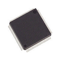
M30626FHPGP Renesas Electronics America, M30626FHPGP Datasheet - Page 67

M30626FHPGP
Manufacturer Part Number
M30626FHPGP
Description
Manufacturer
Renesas Electronics America
Datasheet
1.M30626FHPGP.pdf
(103 pages)
Specifications of M30626FHPGP
Cpu Family
M16C
Device Core Size
16/32Bit
Frequency (max)
24MHz
Interface Type
I2C/IEBus/UART
Program Memory Type
Flash
Program Memory Size
384KB
Total Internal Ram Size
31KB
# I/os (max)
87
Number Of Timers - General Purpose
11
Operating Supply Voltage (typ)
5V
Operating Supply Voltage (max)
5.5V
Operating Supply Voltage (min)
3.3V
On-chip Adc
26-chx10-bit
On-chip Dac
2-chx8-bit
Instruction Set Architecture
CISC
Operating Temp Range
-20C to 85C
Operating Temperature Classification
Commercial
Mounting
Surface Mount
Pin Count
100
Package Type
LQFP
Lead Free Status / Rohs Status
Compliant
Available stocks
Company
Part Number
Manufacturer
Quantity
Price
Company:
Part Number:
M30626FHPGP
Manufacturer:
RENESAS
Quantity:
24
Part Number:
M30626FHPGP
Manufacturer:
RENESAS/瑞萨
Quantity:
20 000
Company:
Part Number:
M30626FHPGP#U3C
Manufacturer:
Renesas
Quantity:
300
Company:
Part Number:
M30626FHPGP#U3C
Manufacturer:
Renesas
Quantity:
834
Company:
Part Number:
M30626FHPGP#U3C
Manufacturer:
Renesas Electronics America
Quantity:
10 000
Part Number:
M30626FHPGP#U5
Manufacturer:
RENESAS/瑞萨
Quantity:
20 000
Company:
Part Number:
M30626FHPGP#U5C
Manufacturer:
Renesas Electronics America
Quantity:
10 000
Part Number:
M30626FHPGP#U5C
Manufacturer:
RENESAS/瑞萨
Quantity:
20 000
Company:
Part Number:
M30626FHPGP#U7C
Manufacturer:
Renesas Electronics America
Quantity:
10 000
M16C/62P Group (M16C/62P, M16C/62PT)
Rev.2.41
REJ03B0001-0241
Table 5.30
NOTES:
V
V
V
V
V
V
I
I
R
R
R
V
Symbol
IH
IL
OH
OH
OL
OL
T+-
T+-
RAM
PULLUP
fXIN
fXCIN
1. Referenced to V
2. V
3. There is no external connections for port P1_0 to P1_7, P4_4 to P4_7, P7_2 to P7_5 and P9_1 in 80-pin version.
V
V
T-
T-
otherwise specified.
CC1
Jan 10, 2006
HIGH Output
Voltage
HIGH Output Voltage
HIGH Output Voltage
LOW Output
Voltage
LOW Output Voltage
LOW Output Voltage
Hysteresis
Hysteresis
HIGH Input
Current
LOW Input
Current
Pull-Up
Resistance
(3)
Feedback Resistance XIN
Feedback Resistance XCIN
RAM Retention Voltage
for the port P6 to P11 and P14, and V
(3)
(3)
Electrical Characteristics (1)
(3)
(3)
CC1
P6_0 to P6_7, P7_2 to P7_7, P8_0 to P8_4,
P8_6, P8_7, P9_0 to P9_7, P10_0 to P10_7,
P11_0 to P11_7, P14_0, P14_1
P0_0 to P0_7, P1_0 to P1_7, P2_0 to P2_7,
P3_0 to P3_7, P4_0 to P4_7, P5_0 to P5_7,
P12_0 to P12_7, P13_0 to P13_7
P6_0 to P6_7, P7_0 to P7_7, P8_0 to P8_4,
P8_6, P8_7, P9_0 to P9_7, P10_0 to P10_7,
P11_0 to P11_7, P14_0, P14_1
P0_0 to P0_7, P1_0 to P1_7, P2_0 to P2_7,
P3_0 to P3_7, P4_0 to P4_7, P5_0 to P5_7,
P12_0 to P12_7, P13_0 to P13_7
HOLD, RDY, TA0IN to TA4IN,
TB0IN to TB5IN, INT0 to INT5, NMI,
ADTRG, CTS0 to CTS2, CLK0 to CLK4,
TA0OUT to TA4OUT, KI0 to KI3, RXD0 to RXD2,
SCL0 to SCL2, SDA0 to SDA2, SIN3, SIN4
RESET
P0_0 to P0_7, P1_0 to P1_7, P2_0 to P2_7,
P3_0 to P3_7, P4_0 to P4_7, P5_0 to P5_7,
P6_0 to P6_7, P7_0 to P7_7, P8_0 to P8_7,
P9_0 to P9_7, P10_0 to P10_7, P11_0 to P11_7,
P12_0 to P12_7, P13_0 to P13_7, P14_0, P14_1,
XIN, RESET, CNVSS, BYTE
P0_0 to P0_7, P1_0 to P1_7, P2_0 to P2_7,
P3_0 to P3_7, P4_0 to P4_7, P5_0 to P5_7,
P6_0 to P6_7, P7_0 to P7_7, P8_0 to P8_7,
P9_0 to P9_7, P10_0 to P10_7, P11_0 to P11_7,
P12_0 to P12_7, P13_0 to P13_7, P14_0, P14_1,
XIN, RESET, CNVSS, BYTE
P0_0 to P0_7, P1_0 to P1_7, P2_0 to P2_7, P3_0
to P3_7, P4_0 to P4_7, P5_0 to P5_7, P6_0 to
P6_7, P7_2 to P7_7, P8_0 to P8_4, P8_6, P8_7,
P9_0 to P9_7, P10_0 to P10_7,
P11_0 to P11_7,P12_0 to P12_7, P13_0 to P13_7,
P14_0, P14_1
= V
Page 65 of 96
CC2
XOUT
XCOUT
XOUT
XCOUT
Parameter
= 2.7 to 3.3V, V
HIGHPOWER
LOWPOWER
HIGHPOWER
LOWPOWER
HIGHPOWER
LOWPOWER
HIGHPOWER
LOWPOWER
CC2
SS
= 0V at Topr = − 20 to 85 ° C / − 40 to 85 ° C, f(XIN)=10MHz no wait unless
for the port P0 to P5 and P12 to P13
(1)
I
I
I
I
With no load applied
With no load applied
I
I
I
I
With no load applied
With no load applied
V
V
V
At stop mode
OH
OH
OH
OH
OL
OL
OL
OL
I
I
I
=3V
=0V
=0V
Measuring Condition
=1mA
=1mA
=0.1mA
=50
=
=
=
=
−
−
−0.
−
1mA
1mA
50
µ
1mA
A
µ
(2)
A
(2)
V
V
V
V
V
CC1
CC2
CC1
CC1
CC1
5. Electrical Characteristics
Min.
0.2
0.2
2.0
50
− 0.5
− 0.5
− 0.5
− 0.5
Standard
=V
(0.7)
Typ.
100
2.5
1.6
3.0
25
0
0
CC2
Max.
V
V
V
V
− 4.0
500
0.5
0.5
0.5
0.5
0.8
1.8
4.0
CC1
CC2
CC1
CC1
=3V
Unit
M Ω
M Ω
µ A
µ A
k Ω
V
V
V
V
V
V
V
V
V


