PHB45N03LT NXP Semiconductors, PHB45N03LT Datasheet
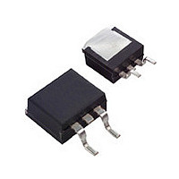
PHB45N03LT

Manufacturer Part Number
PHB45N03LT
Description
Manufacturer
NXP Semiconductors
Type
Power MOSFETr
Datasheet

Specifications of PHB45N03LT

Number Of Elements
1
Polarity
N
Channel Mode
Enhancement
Drain-source On-res
0.021Ohm
Drain-source On-volt
30V
Gate-source Voltage (max)
±15V
Continuous Drain Current
45A
Power Dissipation
86W
Operating Temp Range
-55C to 175C
Operating Temperature Classification
Military
Mounting
Surface Mount
Pin Count
2 +Tab
Package Type
D2PAK
Lead Free Status / Rohs Status
Not Compliant

Available stocks

Company
Part Number
Manufacturer
Quantity
Price
Part Number:
PHB45N03LT
Manufacturer:
PH
Quantity:
640
Part Number:
PHB45N03LT
Manufacturer:
PHILIPS/飞利浦
Quantity:
20 000
Part Number:
PHB45N03LT
Manufacturer:
PHI
Quantity:
10 120
Philips Semiconductors
FEATURES
• ’Trench’ technology
• Very low on-state resistance
• Fast switching
• Stable off-state characteristics
• High thermal cycling performance
• Low thermal resistance
GENERAL DESCRIPTION
N-channel enhancement mode logic level field-effect power transistor in a plastic envelope using ’trench’ technology.
The device has very low on-state resistance. It is intended for use in dc to dc converters and general purpose switching
applications.
The PHP45N03LT is supplied in the SOT78 (TO220AB) conventional leaded package.
The PHB45N03LT is supplied in the SOT404 surface mounting package.
The PHD45N03LT is supplied in the SOT428 surface mounting package.
PINNING
LIMITING VALUES
Limiting values in accordance with the Absolute Maximum System (IEC 134)
1 It is not possible to make connection to pin 2 of the SOT428 or SOT404 packages.
January 1998
TrenchMOS
Logic level FET
SYMBOL PARAMETER
V
V
V
I
I
P
T
D
DM
j
DSS
DGR
GS
D
PIN
, T
tab
1
2
3
stg
gate
drain
source
drain
DESCRIPTION
Drain-source voltage
Drain-gate voltage
Gate-source voltage
Continuous drain current
Pulsed drain current
Total power dissipation
Operating junction and
storage temperature
1
transistor
SOT78 (TO220AB)
SYMBOL
tab
CONDITIONS
T
T
T
T
T
T
j
j
mb
mb
mb
mb
1 2 3
= 25 ˚C to 175˚C
= 25 ˚C to 175˚C; R
= 25 ˚C; V
= 100 ˚C; V
= 25 ˚C
= 25 ˚C
g
PHP45N03LT, PHB45N03LT, PHD45N03LT
1
GS
GS
d
s
= 10 V
SOT404
= 10 V
GS
= 20 k
1
tab
2
3
QUICK REFERENCE DATA
R
R
DS(ON)
DS(ON)
MIN.
- 55
SOT428
V
21 m (V
-
-
-
-
-
-
-
24 m (V
I
DSS
D
Product specification
= 45 A
= 30 V
MAX.
180
175
1
30
30
45
33
86
15
tab
GS
2
GS
3
= 10 V)
Rev 1.300
= 5 V)
UNIT
W
˚C
V
V
V
A
A
A

Related parts for PHB45N03LT

PHB45N03LT Summary of contents

Page 1

... The device has very low on-state resistance intended for use converters and general purpose switching applications. The PHP45N03LT is supplied in the SOT78 (TO220AB) conventional leaded package. The PHB45N03LT is supplied in the SOT404 surface mounting package. The PHD45N03LT is supplied in the SOT428 surface mounting package. PINNING ...

Page 2

... Internal drain inductance d L Internal drain inductance d L Internal source inductance s C Input capacitance iss C Output capacitance oss C Feedback capacitance rss January 1998 PHP45N03LT, PHB45N03LT, PHD45N03LT CONDITIONS SOT78 package, in free air SOT404 and SOT428 packages, pcb mounted, minimum footprint CONDITIONS 0.25 mA ...

Page 3

... Reverse recovery charge rr AVALANCHE LIMITING VALUE SYMBOL PARAMETER W Drain-source non-repetitive DSS unclamped inductive turn-off energy Normalised Power Derating PD% 120 110 100 100 Tmb / C Fig.1. Normalised power dissipation. PD% = 100 ˚C January 1998 PHP45N03LT, PHB45N03LT, PHD45N03LT CONDITIONS -dI /dt = 100 - CONDITIONS 120 110 100 90 ...

Page 4

... Fig.4. Transient thermal impedance f(t); parameter j-mb ID, Drain current (Amps VDS, Drain-Source voltage (Volts) Fig.5. Typical output characteristics I = f(V ); parameter January 1998 PHP45N03LT, PHB45N03LT, PHD45N03LT PHP42N03LT 0.06 0. 10us 0.04 100 0.01 100 ms 0 100 p 7528- 1E-01 1E+ ...

Page 5

... Sub-Threshold Conduction 1E-01 1E-02 2% typ 1E-03 1E-04 1E-05 1E-05 0 0.5 1 1.5 Fig.11. Sub-threshold drain current f GS) DS January 1998 PHP45N03LT, PHB45N03LT, PHD45N03LT 30V TrenchMOS 10000 1000 100 100 200 150 0.1 Fig.12. Typical capacitances BUK959- 100 150 200 Fig.13. Typical turn-on gate-charge characteristics. ...

Page 6

... Logic level FET WDSS% 120 110 100 100 120 Tmb / C Fig.15. Normalised avalanche energy rating f DSS mb D January 1998 PHP45N03LT, PHB45N03LT, PHD45N03LT VGS 0 140 160 180 = Product specification L VDS T.U. RGS shunt Fig.16. Avalanche energy test circuit 0 DSS D DSS DSS DD VDD + - -ID/100 Rev 1 ...

Related keywords