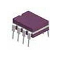
LM6172AMJ-QML National Semiconductor, LM6172AMJ-QML Datasheet - Page 3

LM6172AMJ-QML
Manufacturer Part Number
LM6172AMJ-QML
Description
Manufacturer
National Semiconductor
Type
Voltage Feedback Amplifierr
Datasheet
1.LM6172AMJ-QML.pdf
(21 pages)
Specifications of LM6172AMJ-QML
Rail/rail I/o Type
No
Number Of Elements
2
Unity Gain Bandwidth Product
80MHz
Slew Rate
1700V/us
Common Mode Rejection Ratio
70dB
Input Offset Voltage
1mV
Input Bias Current
2.5uA
Single Supply Voltage (typ)
Not RequiredV
Dual Supply Voltage (typ)
±3/±5/±9/±12/±15V
Power Dissipation
1.03W
Voltage Gain In Db
70dB
Power Supply Rejection Ratio
75dB
Power Supply Requirement
Dual
Shut Down Feature
No
Single Supply Voltage (min)
Not RequiredV
Single Supply Voltage (max)
Not RequiredV
Dual Supply Voltage (min)
±2.75V
Dual Supply Voltage (max)
±18V
Technology
BiCOM
Operating Temp Range
-55C to 125C
Operating Temperature Classification
Military
Mounting
Through Hole
Pin Count
8
Package Type
CDIP
Lead Free Status / Rohs Status
Not Compliant
Available stocks
Company
Part Number
Manufacturer
Quantity
Price
Company:
Part Number:
LM6172AMJ-QML
Manufacturer:
TI
Quantity:
501
MICROCIRCUIT DATA SHEET
MNLM6172AM-X REV 2A1
Applications
(Continued)
LAYOUT CONSIDERATION: Printed Circuit Boards and High Speed Op Amps: There are many things
to consider when designing PC boards for high speed op amps. Without proper caution, it is
very easy to cause excessive ringing, oscillation and to degrade the AC performance in
high speed circuits. As a rule, the signal traces should be short and wide to provide low
inductance and low impedance paths. Any unused board space must be grounded to reduce
stray signal pickup. Critical components should also be grounded at a common point to
eliminate voltage drop. Sockets add capacitance to the board and can affect frequency
performance. It is better to solder the amplifier directly into the PC board without using
any socket.
USING PROBES: Active (FET) probes are ideal for taking high frequency measurements because
they have wide bandwidth, high input impedance, and low input capacitance. However, the
probe ground leads provide a long ground loop that will produce errors in measurement.
Instead, the probes can be grounded directly to the oscilloscope by removing the ground
leads and probe jackets and using scope probe jacks.
COMPONENT SELECTION & FEEDBACK RESISTOR: It is important in high speed applications to
keep all component leads short because wires are inductive at high frequency. For discrete
components, choose carbon composition-type resistors and mica-type capacitors. Surface
mount components are preferred over discrete components for minimum inductive effect.
Large values of feedback resistors can couple with parasitic capacitance and cause
undesirable effects such as ringing or oscillation in high speed amplifiers. For the
LM6172, a feedback resistor of 1k Ohm gives optimal performance.
COMPENSATION FOR INPUT CAPACITANCE: The combination of an amplfier's input capacitance,
with the gain setting resistors, adds a pole that can cause peaking or oscillation. To
solve this problem, a feedback capacitor with a value Cf>(Rg X Cin)/Rf can be used to
cancel that pole. For the LM6172, a feedback capacitor of 2pF is recommended. AN00003
illistrates the compensation circuit.
POWER SUPPLY BYPASSING: Bypassing the power supply is necessary to maintain low power
supply impedance across frequency. Both positive and negative device power supply pins
should be bypassed individually by placing 0.01uF ceramic capacitors directly to the
device supply pins, and 2.2uF tantalum capacitors within 0.25 inch of the power supply
pins. See AN00004.
TERMINATION: In high frequency applications, reflections occur if signals are not properly
terminated. Figure 6, in the Commercial Data Book, shows a properly terminated signal
while, Figure 7, in the Commercial Data Book, shows an improperly terminated signal.
To minimize reflection, coaxial cable, with characteristic impedance matched to the signal
source, should be used. The other end of the cable should be terminated with the same
value terminator or resistor. For the commonly used cables, RG59 has 75 Ohm characteristic
impedance, and RG58 has 50 Ohm characteristic impedance.
DRIVING CAPACITIVE LOADS: Amplifiers driving capacitive loads can oscillate or have
ringing at the output. To eliminate oscillation or reduce ringing, an isolation resistor
can be placed as shown in AN00007. The combination of the isolation resistor and the load
capacitor forms a pole to increase stability by adding more phase margin to the overall
system. The desired performance depends upon the value of the isolation resistor; the
bigger the isolation resistor, the more damped (slow) the pulse response becomes. For
LM6172, a 50 Ohm isolation resistor is recommended for initial evaluation.
POWER DISSIPATION: The maximum power allowed to dissipate in a device is defined as:
Pd=(Tj(max) - TA)/ThetaJA, where Pd is the power dissipation in a device, Tj(max) is the
maximum junction temperature, TA is the ambient temperature, ThetaJA is the thermal
resistance of a particular package.
For example, for the LM6172 in a J-8 package, the maximum power dissipation at 25 C
ambient temperature is 1030mW.
Thermal resistance, ThetaJA, depends upon parameters such as die size, package size and
package material. The smaller the die size and package, the higher ThetaJA becomes.
The total power dissipation in a device can be calculated as: Pd = Pq + Pl where Pq is the
quiescent power dissipated in a device with no load connected at the output, and Pl is the
power dissipated in the device with a load connected at the output.
Pl is not the power
dissipated by the load.
Furthermore, Pq = supply current x total supply voltage with no load or Is[V+ plus V-].
Pl = output current x (voltage difference between supply voltage and output voltage of the
same supply) or Il[V+ - Vo].
For example, the total power dissipated by the LM6172 with Vs = +15V with both amplifiers
swinging output voltage of 10V into 1k Ohm is:
3


