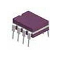
LM6172AMJ-QML National Semiconductor, LM6172AMJ-QML Datasheet - Page 5

LM6172AMJ-QML
Manufacturer Part Number
LM6172AMJ-QML
Description
Manufacturer
National Semiconductor
Type
Voltage Feedback Amplifierr
Datasheet
1.LM6172AMJ-QML.pdf
(21 pages)
Specifications of LM6172AMJ-QML
Rail/rail I/o Type
No
Number Of Elements
2
Unity Gain Bandwidth Product
80MHz
Slew Rate
1700V/us
Common Mode Rejection Ratio
70dB
Input Offset Voltage
1mV
Input Bias Current
2.5uA
Single Supply Voltage (typ)
Not RequiredV
Dual Supply Voltage (typ)
±3/±5/±9/±12/±15V
Power Dissipation
1.03W
Voltage Gain In Db
70dB
Power Supply Rejection Ratio
75dB
Power Supply Requirement
Dual
Shut Down Feature
No
Single Supply Voltage (min)
Not RequiredV
Single Supply Voltage (max)
Not RequiredV
Dual Supply Voltage (min)
±2.75V
Dual Supply Voltage (max)
±18V
Technology
BiCOM
Operating Temp Range
-55C to 125C
Operating Temperature Classification
Military
Mounting
Through Hole
Pin Count
8
Package Type
CDIP
Lead Free Status / Rohs Status
Not Compliant
Available stocks
Company
Part Number
Manufacturer
Quantity
Price
Company:
Part Number:
LM6172AMJ-QML
Manufacturer:
TI
Quantity:
501
MNLM6172AM-X REV 2A1
Supply Voltage (V+ - V-)
Differential Input Voltage
Maximum Junction Temperature
Power Dissipation
Output Short Circuit to Ground
Operating Temperature Range
Storage Temperature Range
Thermal Resistance
Package Weight
ESD Tolerance
Note 1:
Note 2:
Note 3:
(Note 6)
(Note 2, 3)
(Note 4)
(Note 7)
(Note 5)
(Absolute Maximum Ratings)
(Note 1)
ThetaJA
ThetaJC
(Typical)
Human Body Model
CERAMIC SOIC
CERAMIC DIP
CERAMIC SOIC
(Note 3)
8-Pin CERAMIC DIP (Still Air)
CERAMIC SOIC
8-Pin CERAMIC DIP
Absolute Maximum Ratings indicate limits beyond which damage to the device may occur.
Operating Ratings indicate conditions for which the device is functional, but do not
guarantee specific performance limits. For guaranteed specifications and test
conditions, see the Electrical Characteristics. The guaranteed specifications apply
only for the test conditions listed. Some performance characteristics may degrade
when the device is not operated under the listed test conditions.
The maximum power dissipation must be derated at elevated temperatures and is
dictated by Tjmax (maximum junction temperature), ThetaJA (package junction to
ambient thermal resistance), and TA (ambient temperature). The maximum allowable
power dissipation at any temperature is Pdmax = (Tjmax - TA)/ThetaJA or the number
given in the Absolute Maximum Ratings, whichever is lower.
The package material for these devices allows much improved heat transfer over our
standard ceramic packages. In order to take full advantage of this improved heat
transfer, heat sinking must be provided between the package base (directly beneath
the die), and either metal traces on, or thermal vias through, the printed circuit
board. Without this additional heat sinking, device power dissipation must be
calculated using junction-to-ambient, rather than junction-to-case, thermal
resistance. It must not be assumed that the device leads will provide substantial
heat transfer out of the package, since the thermal resistance of the leadframe
material is very poor, relative to the material of the package base. The stated
junction-to-case thermal resistance is for the package material only, and does not
account for the additional thermal resistance between the package base and the
printed circuit board. The user must determine the value of the additional thermal
resistance and must combine this with the stated value for the package, to calculate
the total allowed power dissipation for the device.
(500LF/Min Air flow)
(Still Air)
(500LF/Min Air flow)
5
36V
+10V
150 C
1.03W
Continuous
-55 C < Ta < +125 C
-65 C < Ta < +150 C
100 C/W
124 C/W
980mg
365mg
4kV
46 C/W
74 C/W
2 C/W
6 C/W
MICROCIRCUIT DATA SHEET


