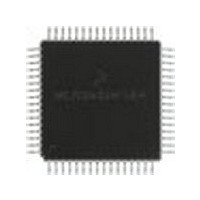
MC68HC11E1CFU3 Freescale Semiconductor, MC68HC11E1CFU3 Datasheet - Page 122

MC68HC11E1CFU3
Manufacturer Part Number
MC68HC11E1CFU3
Description
Manufacturer
Freescale Semiconductor
Datasheet
1.MC68HC11E1CFU3.pdf
(242 pages)
Specifications of MC68HC11E1CFU3
Cpu Family
HC11
Device Core Size
8b
Frequency (max)
3MHz
Interface Type
SCI/SPI
Program Memory Type
ROMLess
Program Memory Size
Not Required
Total Internal Ram Size
512Byte
# I/os (max)
38
Number Of Timers - General Purpose
8
Operating Supply Voltage (typ)
3.3/5V
Operating Supply Voltage (max)
5.5V
Operating Supply Voltage (min)
3V
On-chip Adc
8-chx8-bit
Instruction Set Architecture
CISC
Operating Temp Range
-40C to 85C
Operating Temperature Classification
Industrial
Mounting
Surface Mount
Pin Count
64
Package Type
PQFP
Lead Free Status / Rohs Status
Not Compliant
Available stocks
Company
Part Number
Manufacturer
Quantity
Price
Company:
Part Number:
MC68HC11E1CFU3
Manufacturer:
MOT
Quantity:
5 510
Part Number:
MC68HC11E1CFU3
Manufacturer:
MOTOROLA/摩托罗拉
Quantity:
20 000
Serial Peripheral Interface (SPI)
8.5.3 Serial Clock
SCK, an input to a slave device, is generated by the master device and synchronizes data movement in
and out of the device through the MOSI and MISO lines. Master and slave devices are capable of
exchanging a byte of information during a sequence of eight clock cycles.
Four possible timing relationships can be chosen by using control bits CPOL and CPHA in the serial
peripheral control register (SPCR). Both master and slave devices must operate with the same timing.
The SPI clock rate select bits, SPR[1:0], in the SPCR of the master device, select the clock rate. In a slave
device, SPR[1:0] have no effect on the operation of the SPI.
8.5.4 Slave Select
The slave select (SS) input of a slave device must be externally asserted before a master device can
exchange data with the slave device. SS must be low before data transactions and must stay low for the
duration of the transaction.
The SS line of the master must be held high. If it goes low, a mode fault error flag (MODF) is set in the
serial peripheral status register (SPSR). To disable the mode fault circuit, write a 1 in bit 5 of the port D
data direction register. This sets the SS pin to act as a general-purpose output rather than the dedicated
input to the slave select circuit, thus inhibiting the mode fault flag. The other three lines are dedicated to
the SPI whenever the serial peripheral interface is on.
The state of the master and slave CPHA bits affects the operation of SS. CPHA settings should be
identical for master and slave. When CPHA = 0, the shift clock is the OR of SS with SCK. In this clock
phase mode, SS must go high between successive characters in an SPI message. When CPHA = 1, SS
can be left low between successive SPI characters. In cases where there is only one SPI slave MCU, its
SS line can be tied to V
as long as only CPHA = 1 clock mode is used.
SS
8.6 SPI System Errors
Two system errors can be detected by the SPI system. The first type of error arises in a multiple-master
system when more than one SPI device simultaneously tries to be a master. This error is called a mode
fault. The second type of error, write collision, indicates that an attempt was made to write data to the
SPDR while a transfer was in progress.
When the SPI system is configured as a master and the SS input line goes to active low, a mode fault
error has occurred — usually because two devices have attempted to act as master at the same time. In
cases where more than one device is concurrently configured as a master, there is a chance of contention
between two pin drivers. For push-pull CMOS drivers, this contention can cause permanent damage. The
mode fault mechanism attempts to protect the device by disabling the drivers. The MSTR control bit in the
SPCR and all four DDRD control bits associated with the SPI are cleared and an interrupt is generated
subject to masking by the SPIE control bit and the I bit in the CCR.
Other precautions may need to be taken to prevent driver damage. If two devices are made masters at
the same time, mode fault does not help protect either one unless one of them selects the other as slave.
The amount of damage possible depends on the length of time both devices attempt to act as master.
A write collision error occurs if the SPDR is written while a transfer is in progress. Because the SPDR is
not double buffered in the transmit direction, writes to SPDR cause data to be written directly into the SPI
shift register. Because this write corrupts any transfer in progress, a write collision error is generated. The
transfer continues undisturbed, and the write data that caused the error is not written to the shifter.
M68HC11E Family Data Sheet, Rev. 5.1
122
Freescale Semiconductor


