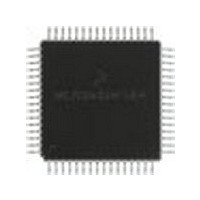
MC68HC11E1CFU3 Freescale Semiconductor, MC68HC11E1CFU3 Datasheet - Page 135

MC68HC11E1CFU3
Manufacturer Part Number
MC68HC11E1CFU3
Description
Manufacturer
Freescale Semiconductor
Datasheet
1.MC68HC11E1CFU3.pdf
(242 pages)
Specifications of MC68HC11E1CFU3
Cpu Family
HC11
Device Core Size
8b
Frequency (max)
3MHz
Interface Type
SCI/SPI
Program Memory Type
ROMLess
Program Memory Size
Not Required
Total Internal Ram Size
512Byte
# I/os (max)
38
Number Of Timers - General Purpose
8
Operating Supply Voltage (typ)
3.3/5V
Operating Supply Voltage (max)
5.5V
Operating Supply Voltage (min)
3V
On-chip Adc
8-chx8-bit
Instruction Set Architecture
CISC
Operating Temp Range
-40C to 85C
Operating Temperature Classification
Industrial
Mounting
Surface Mount
Pin Count
64
Package Type
PQFP
Lead Free Status / Rohs Status
Not Compliant
Available stocks
Company
Part Number
Manufacturer
Quantity
Price
Company:
Part Number:
MC68HC11E1CFU3
Manufacturer:
MOT
Quantity:
5 510
Part Number:
MC68HC11E1CFU3
Manufacturer:
MOTOROLA/摩托罗拉
Quantity:
20 000
- Current page: 135 of 242
- Download datasheet (2Mb)
9.4.2 Timer Compare Force Register
The CFORC register allows forced early compares. FOC[1:5] correspond to the five output compares.
These bits are set for each output compare that is to be forced. The action taken as a result of a forced
compare is the same as if there were a match between the OCx register and the free-running counter,
except that the corresponding interrupt status flag bits are not set. The forced channels trigger their
programmed pin actions to occur at the next timer count transition after the write to CFORC.
The CFORC bits should not be used on an output compare function that is programmed to toggle its
output on a successful compare because a normal compare that occurs immediately before or after the
force can result in an undesirable operation.
Freescale Semiconductor
Register name: Timer Output Compare 3 Register (High)
Register name: Timer Output Compare 3 Register (Low)
Register name: Timer Output Compare 4 Register (High)
Register name: Timer Output Compare 4 Register (Low)
Address:
Reset:
Reset:
Reset:
Reset:
Reset:
Read:
Read:
Read:
Read:
Read:
Write:
Write:
Write:
Write:
Write:
Figure 9-10. Timer Output Compare 3 Register Pair (TOC3)
Figure 9-11. Timer Output Compare 4 Register Pair (TOC4)
$100B
Bit 15
Bit 15
FOC1
Figure 9-12. Timer Compare Force Register (CFORC)
Bit 7
Bit 7
Bit 7
Bit 7
Bit 7
Bit 7
Bit 7
1
1
1
1
0
= Unimplemented
FOC2
Bit 14
Bit 14
Bit 6
Bit 6
1
1
1
1
6
6
6
6
6
0
M68HC11E Family Data Sheet, Rev. 5.1
FOC3
Bit 13
Bit 13
Bit 5
Bit 5
5
1
5
1
5
1
5
1
5
0
FOC4
Bit 12
Bit 12
Bit 4
Bit 4
4
1
4
1
4
1
4
1
4
0
Address: $101B
Address: $101D
Address: $101A
Address: $101C
FOC5
Bit 11
Bit 11
Bit 3
Bit 3
3
1
3
1
3
1
3
1
3
0
Bit 10
Bit 10
Bit 2
Bit 2
2
1
2
1
2
1
2
1
2
0
Bit 9
Bit 1
Bit 9
Bit 1
1
1
1
1
1
1
1
1
1
0
Bit 0
Bit 8
Bit 0
Bit 0
Bit 0
Bit 8
Bit 0
Bit 0
Bit 0
1
1
1
1
0
Output Compare
135
Related parts for MC68HC11E1CFU3
Image
Part Number
Description
Manufacturer
Datasheet
Request
R

Part Number:
Description:
MC68HC11 EEPROM Programming from a Personal Computer
Manufacturer:
Motorola / Freescale Semiconductor
Part Number:
Description:
Manufacturer:
Freescale Semiconductor, Inc
Datasheet:
Part Number:
Description:
Manufacturer:
Freescale Semiconductor, Inc
Datasheet:
Part Number:
Description:
Manufacturer:
Freescale Semiconductor, Inc
Datasheet:
Part Number:
Description:
Manufacturer:
Freescale Semiconductor, Inc
Datasheet:
Part Number:
Description:
Manufacturer:
Freescale Semiconductor, Inc
Datasheet:
Part Number:
Description:
Manufacturer:
Freescale Semiconductor, Inc
Datasheet:
Part Number:
Description:
Manufacturer:
Freescale Semiconductor, Inc
Datasheet:
Part Number:
Description:
Manufacturer:
Freescale Semiconductor, Inc
Datasheet:
Part Number:
Description:
Manufacturer:
Freescale Semiconductor, Inc
Datasheet:
Part Number:
Description:
Manufacturer:
Freescale Semiconductor, Inc
Datasheet:
Part Number:
Description:
Manufacturer:
Freescale Semiconductor, Inc
Datasheet:
Part Number:
Description:
Manufacturer:
Freescale Semiconductor, Inc
Datasheet:
Part Number:
Description:
Manufacturer:
Freescale Semiconductor, Inc
Datasheet:
Part Number:
Description:
Manufacturer:
Freescale Semiconductor, Inc
Datasheet:


