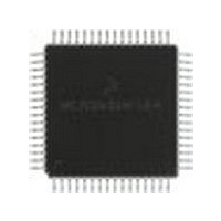
MC68HC11E1CFU3 Freescale Semiconductor, MC68HC11E1CFU3 Datasheet - Page 28

MC68HC11E1CFU3
Manufacturer Part Number
MC68HC11E1CFU3
Description
Manufacturer
Freescale Semiconductor
Datasheet
1.MC68HC11E1CFU3.pdf
(242 pages)
Specifications of MC68HC11E1CFU3
Cpu Family
HC11
Device Core Size
8b
Frequency (max)
3MHz
Interface Type
SCI/SPI
Program Memory Type
ROMLess
Program Memory Size
Not Required
Total Internal Ram Size
512Byte
# I/os (max)
38
Number Of Timers - General Purpose
8
Operating Supply Voltage (typ)
3.3/5V
Operating Supply Voltage (max)
5.5V
Operating Supply Voltage (min)
3V
On-chip Adc
8-chx8-bit
Instruction Set Architecture
CISC
Operating Temp Range
-40C to 85C
Operating Temperature Classification
Industrial
Mounting
Surface Mount
Pin Count
64
Package Type
PQFP
Lead Free Status / Rohs Status
Not Compliant
Available stocks
Company
Part Number
Manufacturer
Quantity
Price
Company:
Part Number:
MC68HC11E1CFU3
Manufacturer:
MOT
Quantity:
5 510
Part Number:
MC68HC11E1CFU3
Manufacturer:
MOTOROLA/摩托罗拉
Quantity:
20 000
- Current page: 28 of 242
- Download datasheet (2Mb)
General Description
1.4.15 Port D
Pins PD5–PD0 can be used for general-purpose I/O signals. These pins alternately serve as the serial
communication interface (SCI) and serial peripheral interface (SPI) signals when those subsystems are
enabled.
1.4.16 Port E
Use port E for general-purpose or analog-to-digital (A/D) inputs.
28
•
•
•
PD0 is the receive data input (RxD) signal for the SCI.
PD1 is the transmit data output (TxD) signal for the SCI.
PD5–PD2 are dedicated to the SPI:
–
–
–
–
PD2 is the master in/slave out (MISO) signal.
PD3 is the master out/slave in (MOSI) signal.
PD4 is the serial clock (SCK) signal.
PD5 is the slave select (SS) input.
If high accuracy is required for A/D conversions, avoid reading port E during
sampling, as small disturbances can reduce the accuracy of that result.
M68HC11E Family Data Sheet, Rev. 5.1
CAUTION
Freescale Semiconductor
Related parts for MC68HC11E1CFU3
Image
Part Number
Description
Manufacturer
Datasheet
Request
R

Part Number:
Description:
MC68HC11 EEPROM Programming from a Personal Computer
Manufacturer:
Motorola / Freescale Semiconductor
Part Number:
Description:
Manufacturer:
Freescale Semiconductor, Inc
Datasheet:
Part Number:
Description:
Manufacturer:
Freescale Semiconductor, Inc
Datasheet:
Part Number:
Description:
Manufacturer:
Freescale Semiconductor, Inc
Datasheet:
Part Number:
Description:
Manufacturer:
Freescale Semiconductor, Inc
Datasheet:
Part Number:
Description:
Manufacturer:
Freescale Semiconductor, Inc
Datasheet:
Part Number:
Description:
Manufacturer:
Freescale Semiconductor, Inc
Datasheet:
Part Number:
Description:
Manufacturer:
Freescale Semiconductor, Inc
Datasheet:
Part Number:
Description:
Manufacturer:
Freescale Semiconductor, Inc
Datasheet:
Part Number:
Description:
Manufacturer:
Freescale Semiconductor, Inc
Datasheet:
Part Number:
Description:
Manufacturer:
Freescale Semiconductor, Inc
Datasheet:
Part Number:
Description:
Manufacturer:
Freescale Semiconductor, Inc
Datasheet:
Part Number:
Description:
Manufacturer:
Freescale Semiconductor, Inc
Datasheet:
Part Number:
Description:
Manufacturer:
Freescale Semiconductor, Inc
Datasheet:
Part Number:
Description:
Manufacturer:
Freescale Semiconductor, Inc
Datasheet:


